IPS LCD having molecules remained parallel with electric fields applied

a technology of electric field and ips, applied in static indicating devices, instruments, non-linear optics, etc., can solve the problem that the best angle of view cannot be set in the direction normal to the plane of glass substrates, and achieve the effect of wide view angle characteristic, improved response time and transmittan

Inactive Publication Date: 2001-09-04
BOE HYDIS TECH
View PDF4 Cites 76 Cited by
  • Summary
  • Abstract
  • Description
  • Claims
  • Application Information

AI Technical Summary

Benefits of technology

It is therefore an object of the present invention to provide a liquid crystal display device with an IPS mode having wide view angle characteristic and capable of improving response time and transmittance.

Problems solved by technology

A problem associated with the TN mode-LCD described above, is that the best angle of view cannot be set in the direction normal to the plane of the glass substrate.

Method used


Image

  • IPS LCD having molecules remained parallel with electric fields applied
  • IPS LCD having molecules remained parallel with electric fields applied
  • IPS LCD having molecules remained parallel with electric fields applied

Examples


Embodiment Construction

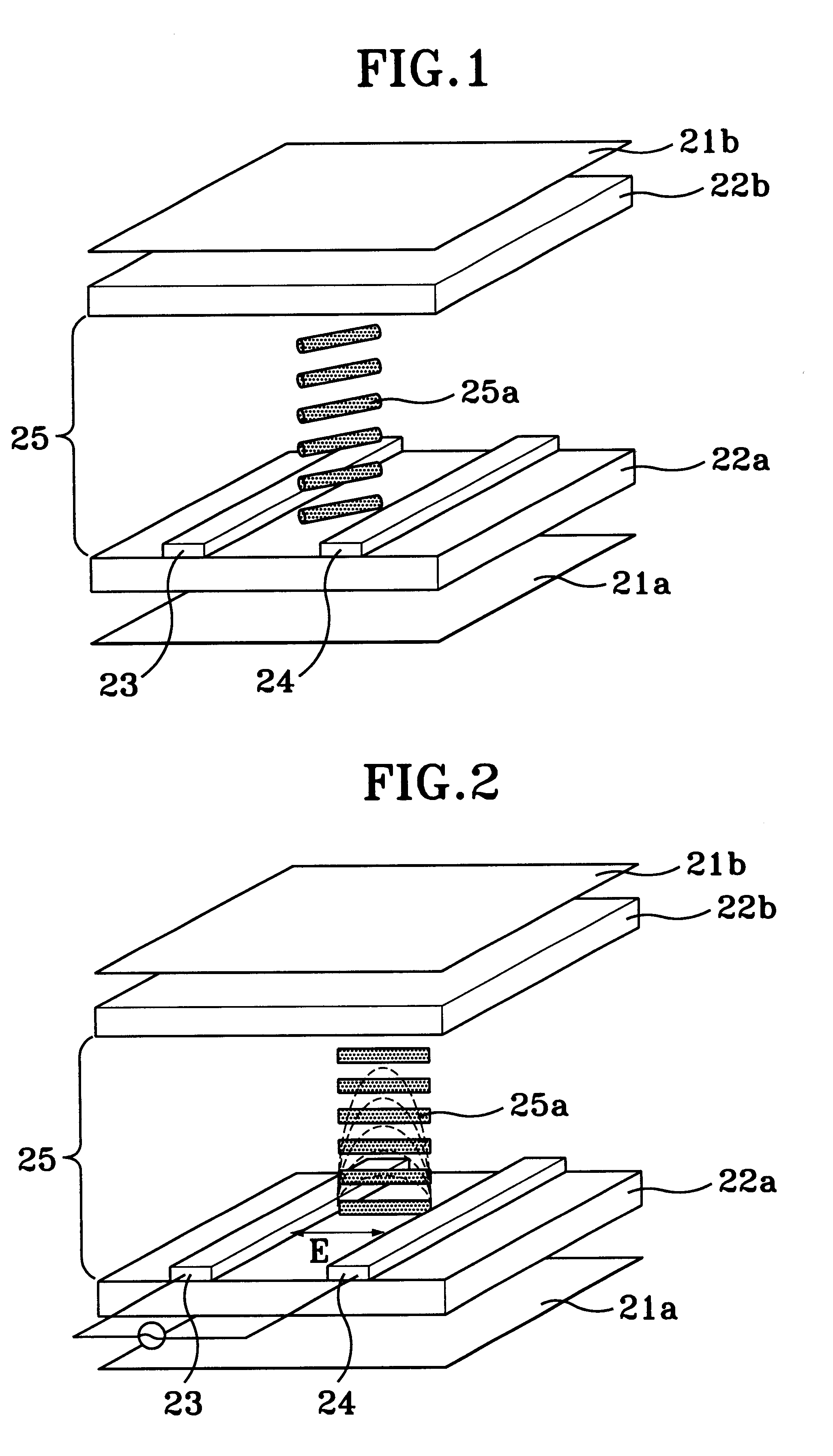
Hereinafter, a preferred embodiment of the present invention will be explained in more detail with reference to the accompanying drawings.

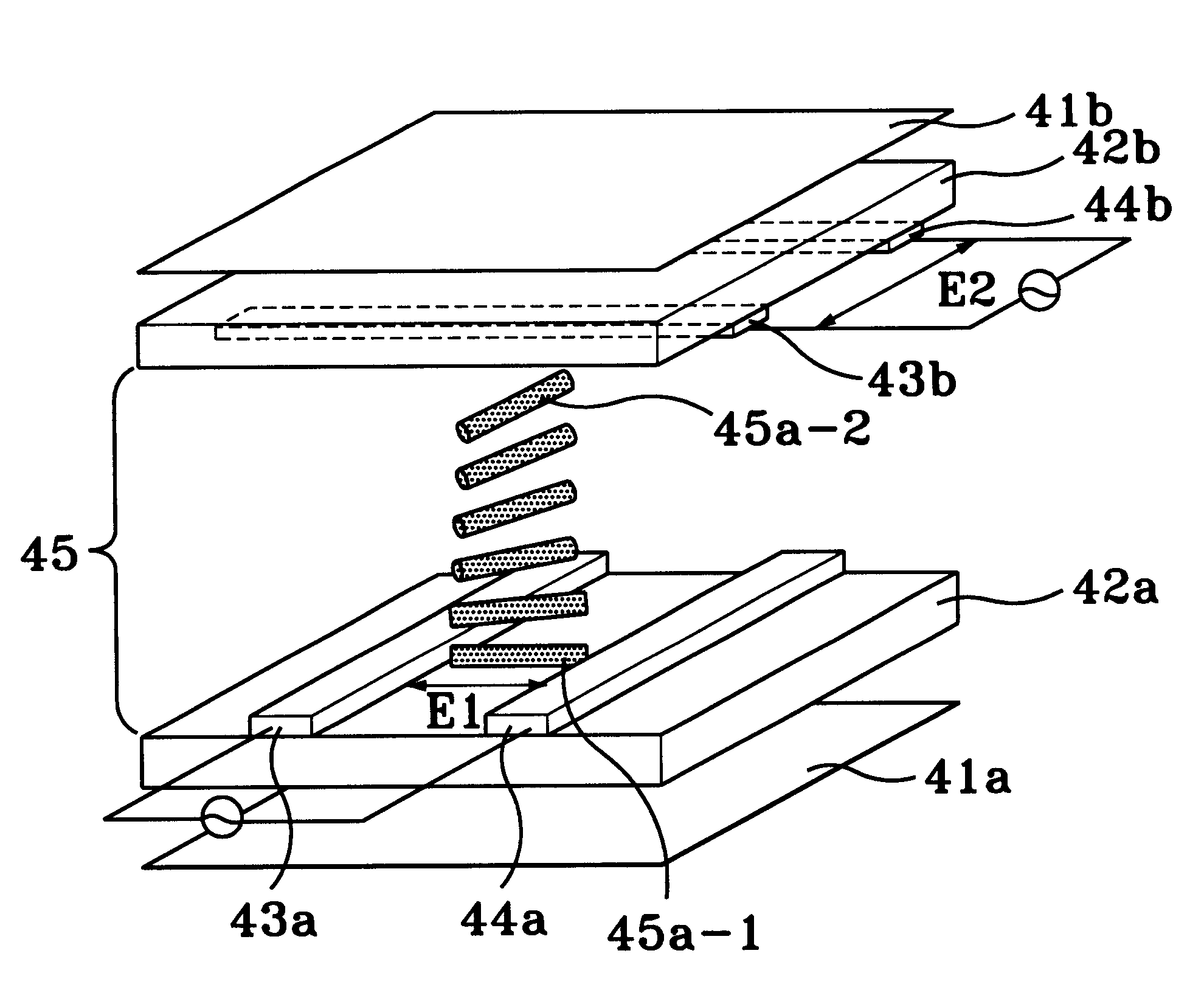
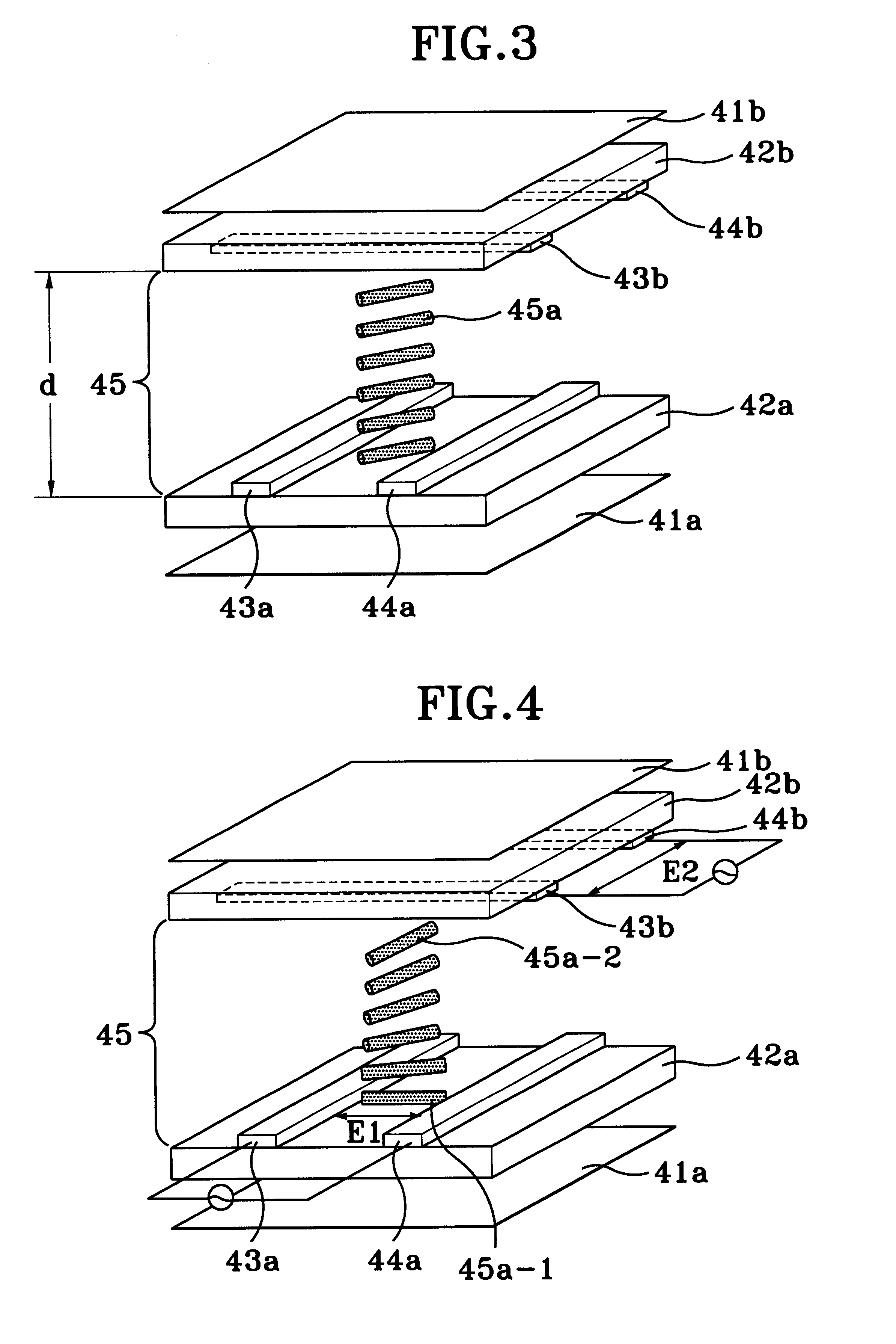
FIG. 3 shows a liquid crystal cell with a IPS mode when a voltage is not applied to the cell, according to an embodiment of the present invention. FIG. 4 shows the liquid crystal cell shown in FIG. 3 when a voltage is applied to the cell.

In FIG. 3, on the outsides of a first and second substrates 42a and 42b, an polarizer 41a and an analyzer 41b are arranged, respectively. The polarization axes of the polarizer 41a and analyzer 41b are orthogonal to each other. On the first substrate 42a, a first pixel electrode 43a and a first counter electrode 44a are formed so that they are spaced with a selected distance and are parallel to each other. On the second substrate 42b, a second pixel electrode 43b and a second counter electrode 44b are also formed so that they are spaced with a selected distance and are parallel to each other. The second pixel elec...


PUM

PropertyMeasurementUnit
angleaaaaaaaaaa
pretilt angleaaaaaaaaaa

Abstract

A liquid crystal display device with an IPS mode having wide view angle characteristic and capable of improving response time and transmittance, is disclosed. A liquid crystal display device with an in-plane switching mode includes a first substrate having first and second electrodes formed thereon. A second substrate is disposed opposite to the first substrate with a selected distance. On a surface of the second substrate are also formed third and fourth electrodes. When a voltage is applied to the respective electrodes, a first electric field which is parallel to the planes of the substrates is generated between the first electrode and the second electrode, and a second electric field which is parallel to the planes of the substrates and is orthogonal to the first electric field is generated between the third electrode and the fourth electrode. A polarizer is arranged on the outside of the first substrate and a analyzer is arranged on the outside of the second substrate. A first homogeneous alignment film is applied to the first substrate on which the first and second electrodes are formed. A second homogeneous alignment film is also applied to the second substrate on which the third and fourth electrodes are formed. A liquid crystal layer having liquid crystal molecules is interposed between the both substrates, wherein the liquid crystal molecules are arranged in a homogeneous state in an absence of the electric field and are twisted in a presence of the electric field.

Description

BACKGROUND OF THE INVENTION1. Field of the InventionThe present invention relates to a liquid crystal display device, and more particularly to a liquid crystal display device with in-plane switching mode.2. Description of the Related ArtOf the various liquid crystal display (LCD) devices, those using the twisted nematic mode (TN mode) have low operation voltage and low power consumption, and in recent years have been widely used. A TN mode cell has a liquid crystal layer interposed between first and second glass substrates on which transparent electrodes are formed. The longitudinal axis of molecules of the liquid crystal are parallel to the planes of the substrates. The first and second glass substrates are arranged for a twist angle of almost 90.degree..A problem associated with the TN mode-LCD described above, is that the best angle of view cannot be set in the direction normal to the plane of the glass substrate. If the direction of the best angle of view from the glass substrat...

Claims


Application Information

Patent Timeline
Patent Type & Authority Patents(United States)
IPC IPC(8): G02F1/13G02F1/1343G02F1/1335G02F1/136G02F1/1337G02F1/1368
CPCG02F1/134363G02F1/1343
Inventor KIM, HYANG YULLEE, SEUNG HEEYOU, JAE GEONPARK, HAN JUN
Owner BOE HYDIS TECH
Why Eureka
Try Eureka