

Substrate of semiconductor device and fabrication method thereof as well as semiconductor device and fabrication method thereof
a semiconductor device and substrate technology, applied in the direction of semiconductor/solid-state device details, instruments, optics, etc., can solve the problems of electrical instability of a thin-film semiconductor, slow operation speed, and low and varied characteristic of the semiconductor devi
- Summary
- Abstract
- Description
- Claims
- Application Information
AI Technical Summary
Problems solved by technology
Method used
Image

Examples
first embodiment
[First Embodiment]
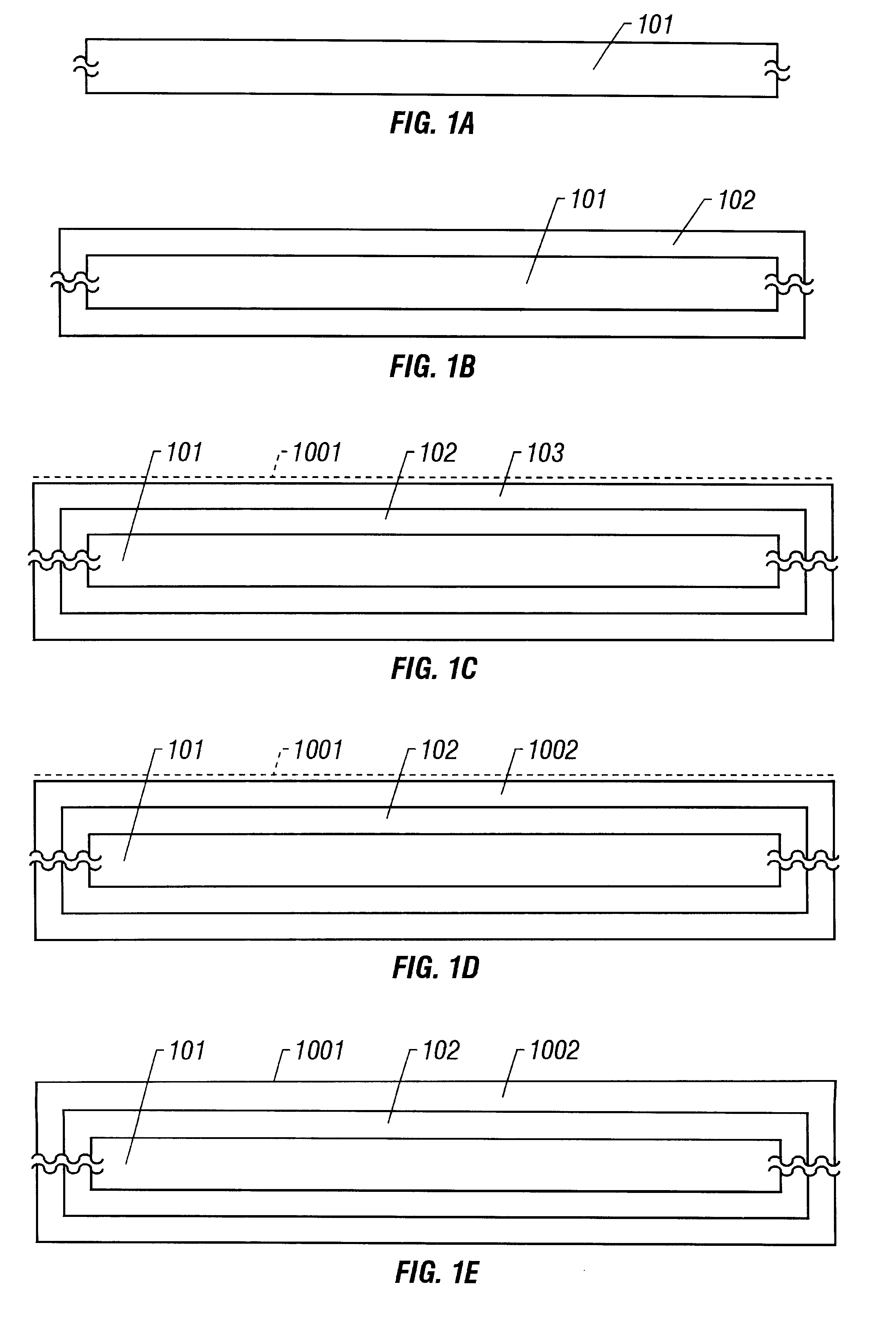
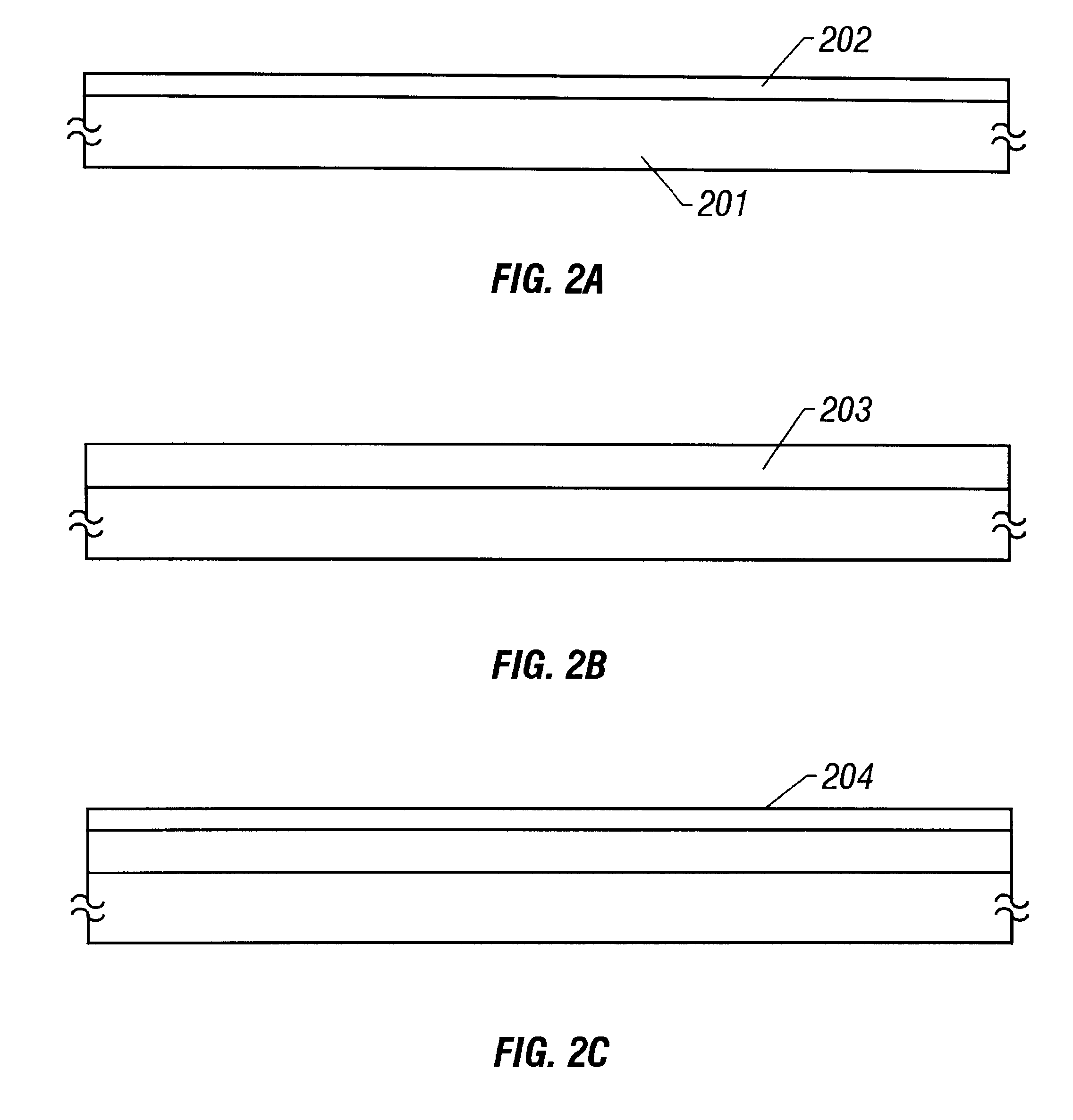
FIGS. 1A through 1E show fabrication steps of the present embodiment. At first, a glass substrate 101 is prepared as shown in FIG. 1A. Although a Corning 1737 glass substrate is used here, other glass substrates such as a Corning 7059 substrate may be used.
Next, a silicon oxide film 102 is deposited so as to have a thickness of 250 nm by means of reduced pressure thermal CVD. Here, the film is deposited by using SiH.sub.4 and NO.sub.2 as original gases and by heating in reduced pressure atmosphere at 600.degree. C. Preferably, the heating temperature is within a range of 600.degree. C..+-.50.degree. C. Thus, a state shown in FIG. 1B is obtained.
In this state, the glass substrate 101 is surrounded by the silicon oxide film 102. That is, the silicon oxide film 102 is deposited on the exposed surrounding surface of the glass substrate.
Precisely speaking, the silicon oxide film 102 is not deposited at the part holding the substrate, so that the glass substrate is not c...
second embodiment
[Second Embodiment]
A case of using a quartz substrate or a crystallized glass substrate as a substrate will be shown in the present embodiment. The outline of steps for fabricating it is basically the same with that shown in FIGS. 1A through 1E.
In the present embodiment, the reduced pressure thermal CVD using SiH.sub.4 and N.sub.2 O as original gases is used as a method for depositing the underlying silicon oxide film.
When SiH.sub.4 and N.sub.2 O are used as original gases, it is preferable to set the deposition temperature at around 850.degree. C.
The arrangement shown in the present embodiment is effective in using a lower grade quartz substrate or a crystallized glass substrate containing much impurity as the substrate.
third embodiment
[Third Embodiment]
A case of using a silicon nitride film, not a silicon oxide film, as the underlying film 102 in the arrangement shown in the first or second embodiment will be shown in the present embodiment. In this case, the reduced pressure thermal CVD is used by using SiH.sub.2 Cl.sub.2 and NH.sub.4 as original gases. At this time, the deposition temperature is set at 600.degree. C. to 850.degree. C.
According to this method, chlorine is contained within the film. Chlorine is effective in fixing movable ions and in suppressing the impurity from moving from the glass substrate.
PUM
| Property | Measurement | Unit |
|---|---|---|
| temperature | aaaaa | aaaaa |
| temperature | aaaaa | aaaaa |
| heat resistance | aaaaa | aaaaa |
Abstract
Description
Claims
Application Information