Contact-less probe of semiconductor wafers

Inactive Publication Date: 2001-10-09
IBM CORP
View PDF14 Cites 33 Cited by
  • Summary
  • Abstract
  • Description
  • Claims
  • Application Information

AI Technical Summary

Problems solved by technology

During the manufacturing of semiconductor devices and wafers, unwanted defects occasionally occur.
By making physical contact with the item being manufactured, the conventional systems introduce

Method used


Image

  • Contact-less probe of semiconductor wafers
  • Contact-less probe of semiconductor wafers
  • Contact-less probe of semiconductor wafers

Examples


Example

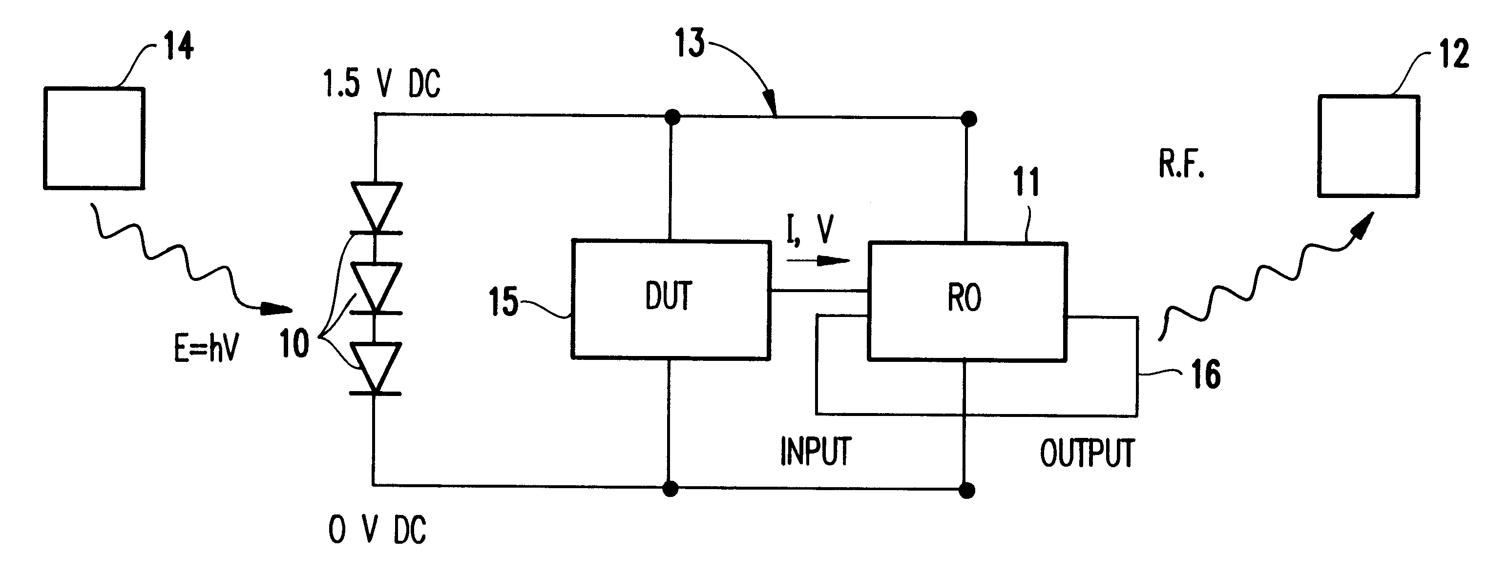
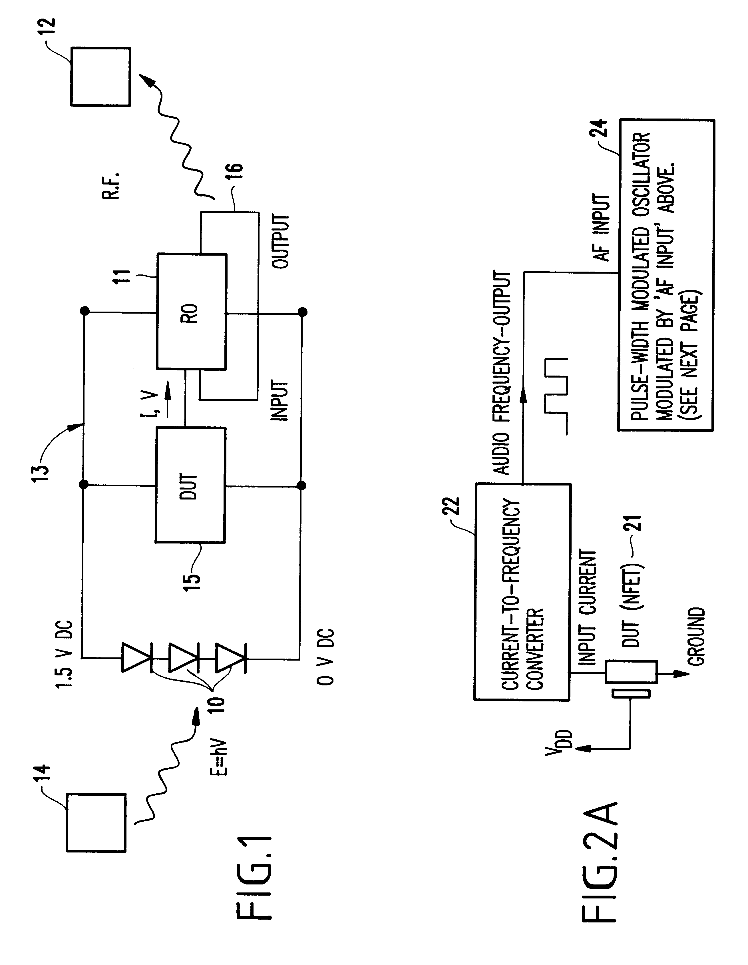
Referring now to the drawings, and more particularly to FIG. 1, a a contact-less probe is illustrated. As mentioned above, the present invention provides a structure and method for determining important device parameters and in-line yield parameters (such as device channel length and metal defects), without physically probing (contacting) the item being manufactured.

The invention includes a light powered generator 10, a radio frequency generator 11, a radio frequency receiver 12, a charge transfer circuit 13 and a light source 14 to power the device under test (DUT) 15, as shown in FIG. 1.

When the DUT 15 is powered by the charge transfer circuit 13, the DUT 15 will send a voltage or current to the radio frequency generator 11 (e.g., ring oscillator). Depending on the DUT output, the radio frequency generator 11 output frequency will vary accordingly.

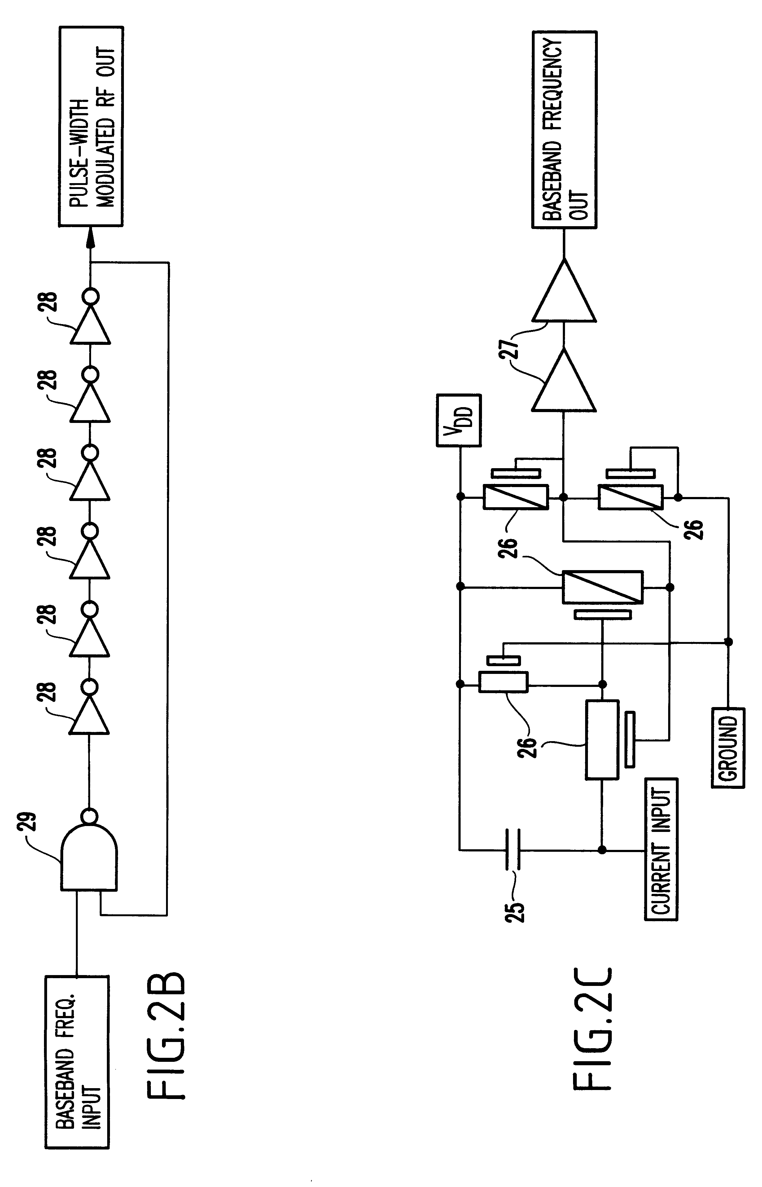
A radio frequency generator is one of the most versatile process and device monitors. For example, a radio frequency generator can be u...


PUM


Abstract

A device, having circuits formed thereon, comprises a circuit including a frequency generator for generating a detectable radio frequency energy when powered and a power generator, coupled to the frequency generator, for generating power when exposed to light.

Description

1. Field of the InventionThe present invention generally relates to devices for testing semiconductor wafers during manufacturing and, more specifically, to testing devices which do not contact the device under test (DUT).2. Description of the Related ArtDuring the manufacturing of semiconductor devices and wafers, unwanted defects occasionally occur. In order to reduce such defects and increase production yield it is desirable to test the item being manufactured at various points during the manufacturing process.Conventional systems remove the item being manufactured from the production line at different fabrication steps and test the item for defects. Depending on the development needs, a semiconductor wafers could be pulled at the post-silicide polysilicon stage, during the local interconnect stage or at several of the metalization stages, such as post metal-1 anneal, post via-1 planarization, or post metal-2 etch, for testing.Conventional testing systems come in physical contact...

Claims


Application Information

Patent Timeline
IPC IPC(8): G01R31/28G01R31/311
CPCG01R31/311Y10S136/291Y10S136/293
Inventor COOK, DONALD J.NOWAK, EDWARD J.TONG, MINH H.
Owner IBM CORP
Why Eureka
Try Eureka