Resist coating and developing unit

a technology of resist coating and developing unit, which is applied in the direction of photosensitive material processing, instruments, printing, etc., can solve the problems of troublesome operation, low system throughput, and difficulty in automatic operation of such operations

Inactive Publication Date: 2001-11-06
TOKYO ELECTRON LTD
View PDF6 Cites 74 Cited by
  • Summary
  • Abstract
  • Description
  • Claims
  • Application Information

AI Technical Summary

Problems solved by technology

Thus, the throughput of the system is low.
Thus, in the conventional system, the operator should perform troublesome operations.
Moreover, it is difficult to automatically perform such operations.

Method used


Image

  • Resist coating and developing unit
  • Resist coating and developing unit
  • Resist coating and developing unit

Examples


Embodiment Construction

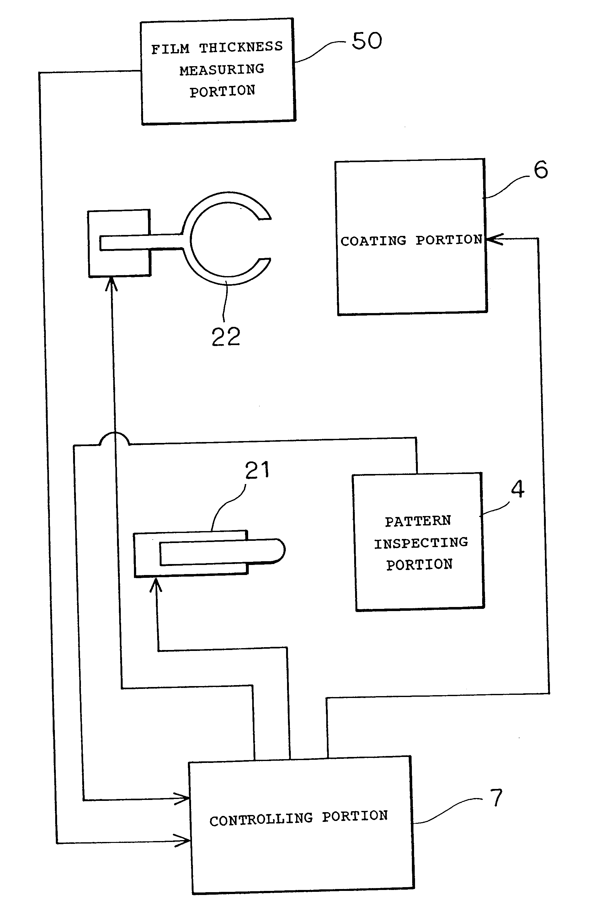
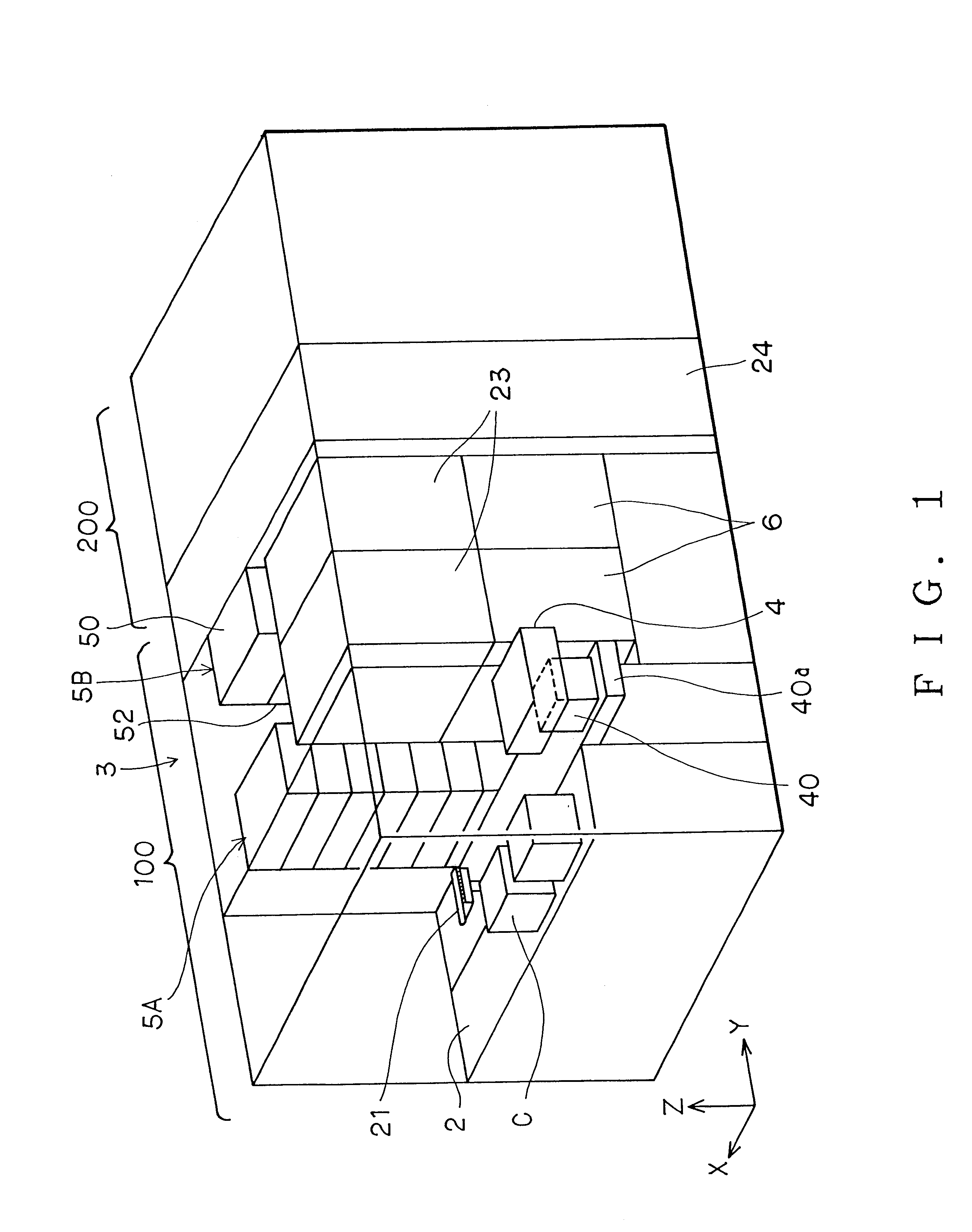
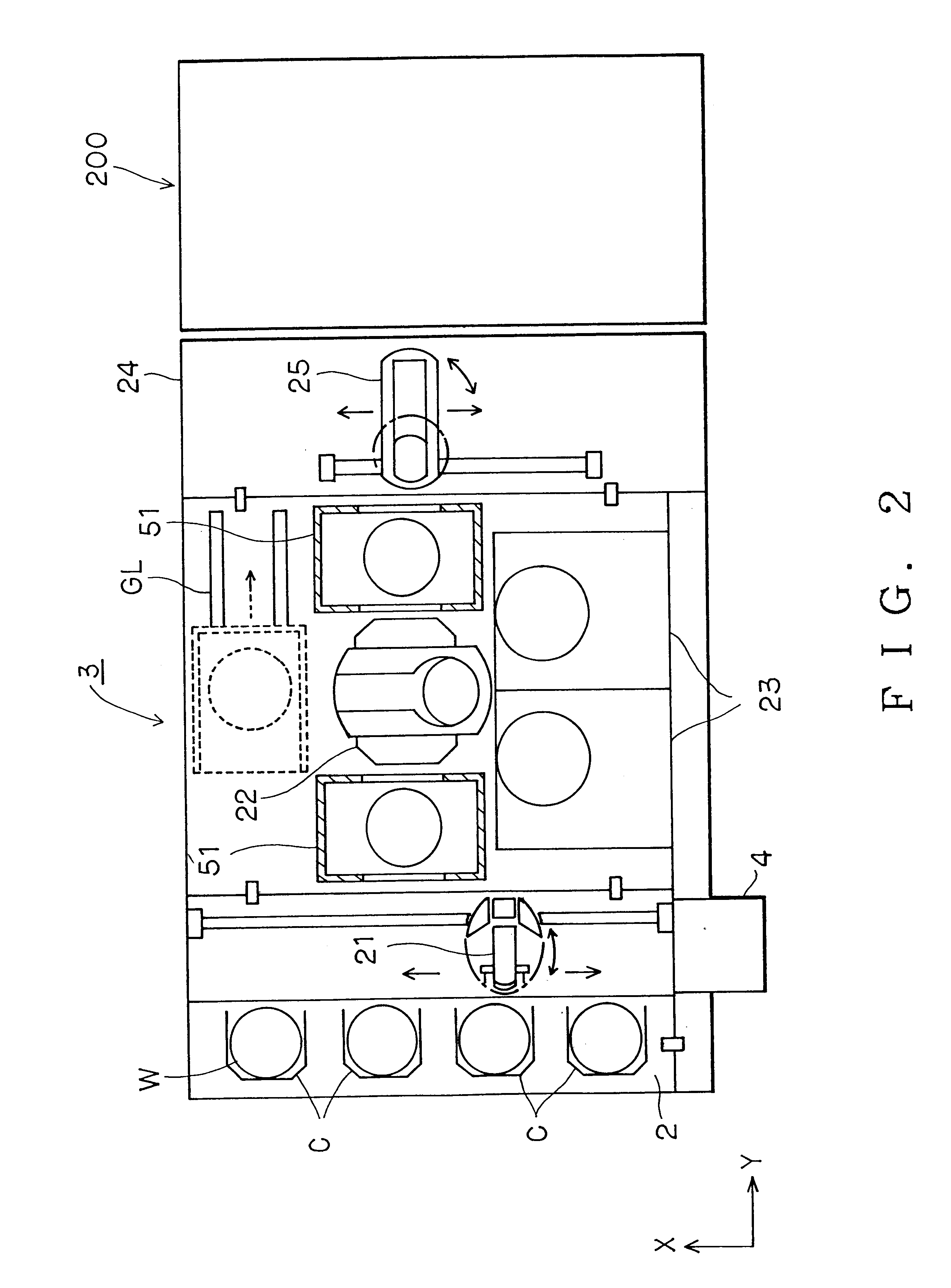
As shown in FIGS. 1 and 2, a coating and developing unit 100 according to an embodiment of the present invention comprises a carrier loading and unloading portion 2, a processing portion 3, and a first wafer transferring portion 21. The carrier loading and unloading portion 2 loads and unloads a wafer carrier C (referred to as carrier) to / from the processing portion 3. The carrier C is a transferring vessel that accommodates a plurality of (for example, 25) wafers W as substrates in a shelf arrangement. The processing portion 3 performs a coating process and a developing process for a wafer W. The first wafer transferring portion 21 transfers a wafer W between the processing portion 3 and the carrier loading and unloading portion 2.

The carrier loading and unloading portion 2 is structured as a stage on which for example four carriers C are placed. The first wafer transferring portion 21 has a pedestal and an arm. The arm that is protrusible and retractable is disposed on the pedesta...


PUM

PropertyMeasurementUnit
thicknessaaaaaaaaaa
widthaaaaaaaaaa
structureaaaaaaaaaa

Abstract

In a transferring region of a wafer transferring portion that transfers a wafer placed in a carrier loading and unloading portion, a pattern inspecting portion for inspecting a resist pattern and a carrier for accommodating a wafer determined as an unacceptable wafer are disposed. The carrier is conveyed to an external cleaning portion. Resist on the unacceptable wafer is cleaned and removed. The resultant wafer is loaded to the coating and developing unit. The film thickness of a monitor wafer is measured by a film thickness measuring portion disposed in the coating and developing unit. Thereafter, resist on the entire surface of the monitor wafer is removed with thinner supplied from a solvent nozzle. Thus, the monitor wafer is regenerated. Consequently, when the coating and developing unit is operated and a substrate and a monitor substrate that have been processes are inspected, the throughput of the coating and developing unit becomes high and the processes can be automatically performed.

Description

1. Field of the InventionThe present invention relates to a resist coating and developing unit for forming a resist film on a substrate, developing a substrate that has been exposed, and forming a desired pattern on the developed substrate.2. Description of the Related ArtIn a fabrication process for a semiconductor device, the photolithography process is used. In the photolithography process, resist solution is coated on a substrate such as a semiconductor wafer. With a photo-mask, the resist film is exposed. The exposed resist film is developed. Thus, a resist mask having a desired pattern is formed on the substrate.The photolithography process is performed by a system of which a coating and developing unit 1A and an exposing unit 1B are connected as shown in FIG. 13. When a semiconductor wafer (hereinafter referred to as wafer) is processed, the coating and developing unit 1A comprises a loading and unloading portion 11, a transferring arm 12, a coating and developing portion 13,...

Claims


Application Information

Patent Timeline
Patent Type & Authority Patents(United States)
IPC IPC(8): H01L21/00G03F7/16G03F7/30H01L21/027H01L21/677
CPCH01L21/67178H01L21/67253
Inventor OGATA, KUNIE
Owner TOKYO ELECTRON LTD
Why Eureka
Try Eureka