

Method and apparatus for automatic routing for reentrant process
a technology of automatic routing and reentry process, applied in the direction of total factory control, programme control, electric programme control, etc., can solve the problem of only updating a few of the settings of the exposure tool
- Summary
- Abstract
- Description
- Claims
- Application Information
AI Technical Summary
Problems solved by technology
Method used
Image

Examples
Embodiment Construction
Illustrative embodiments of the invention are described below. In the interest of clarity, not all features of an actual implementation are described in this specification. It will of course be appreciated that in the development of any such actual embodiment, numerous implementation-specific decisions must be made to achieve the developers' specific goals, such as compliance with system-related and business-related constraints, which will vary from one implementation to another. Moreover, it will be appreciated that such a development effort might be complex and time-consuming but would nevertheless be a routine undertaking for those of ordinary skill in the art having the benefit of this disclosure.
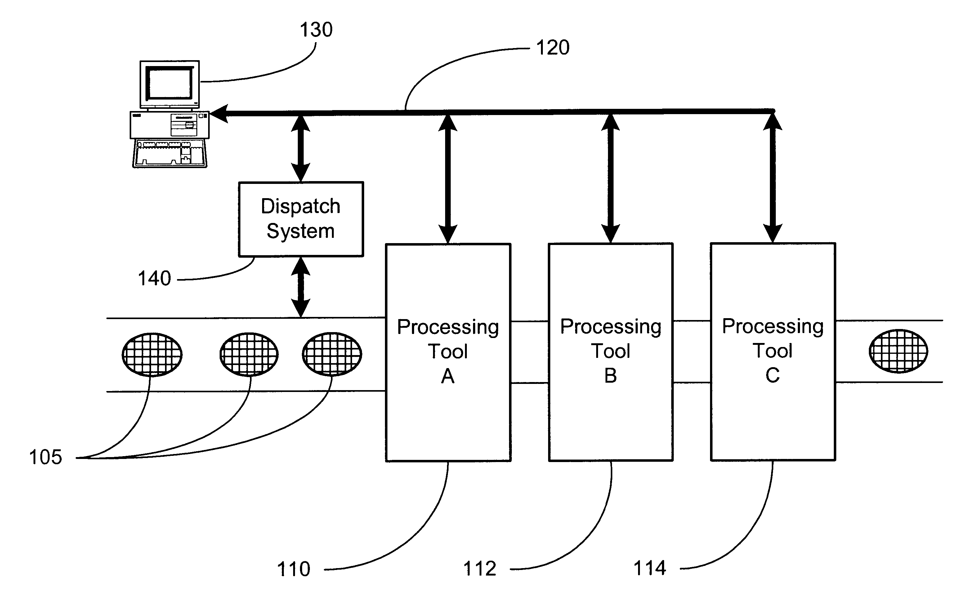
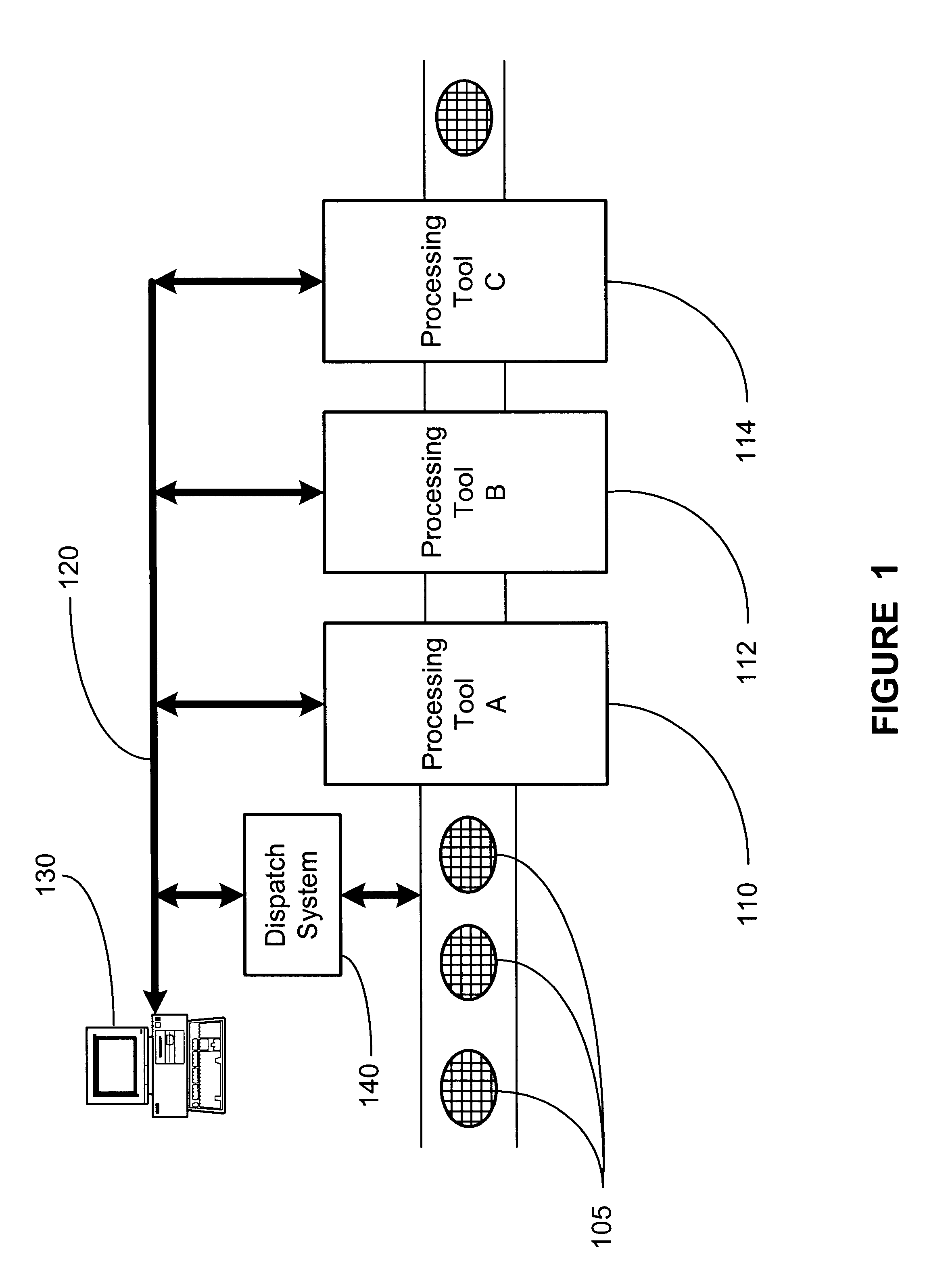
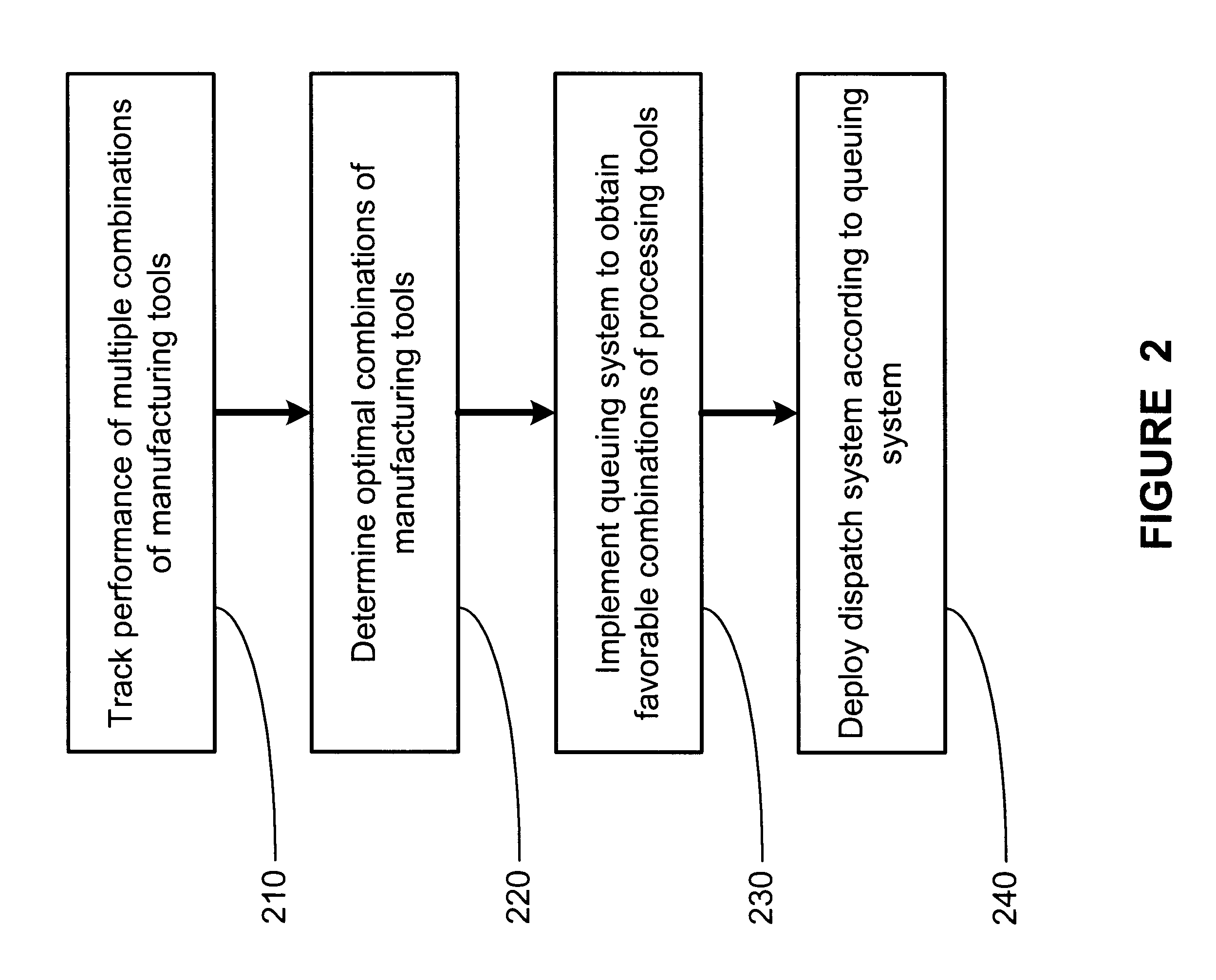
There are many discreet processes that are involved in semiconductor manufacturing. Many times, semiconductor devices are stepped through multiple manufacturing process tools. Some manufacturing process tool combinations produce more favorable results than other combinations. Overlay pr...
PUM
 Abstract
Description
Claims
Application Information