Clock-delayed pseudo-NMOS domino logic

a pseudo-nmos domino logic and clock-delayed technology, applied in logic circuits, pulse techniques, electrical devices, etc., can solve problems such as logic errors, certain functions are difficult to implement, and conventional mos-implemented domino logic is generally limited to non-,

Inactive Publication Date: 2002-04-16
NAN YA TECH
View PDF4 Cites 23 Cited by
  • Summary
  • Abstract
  • Description
  • Claims
  • Application Information

AI Technical Summary

Problems solved by technology

But despite these advantages, domino logic does have certain drawbacks.
For example, where domino logic is implemented using MOS technology, certain functions are difficult to implement because they require the use of inverting logic functions (e.g., NOR, NOT, NAND functions).
Instead, conventional MOS-imp...

Method used


Image

  • Clock-delayed pseudo-NMOS domino logic
  • Clock-delayed pseudo-NMOS domino logic
  • Clock-delayed pseudo-NMOS domino logic

Examples


Embodiment Construction

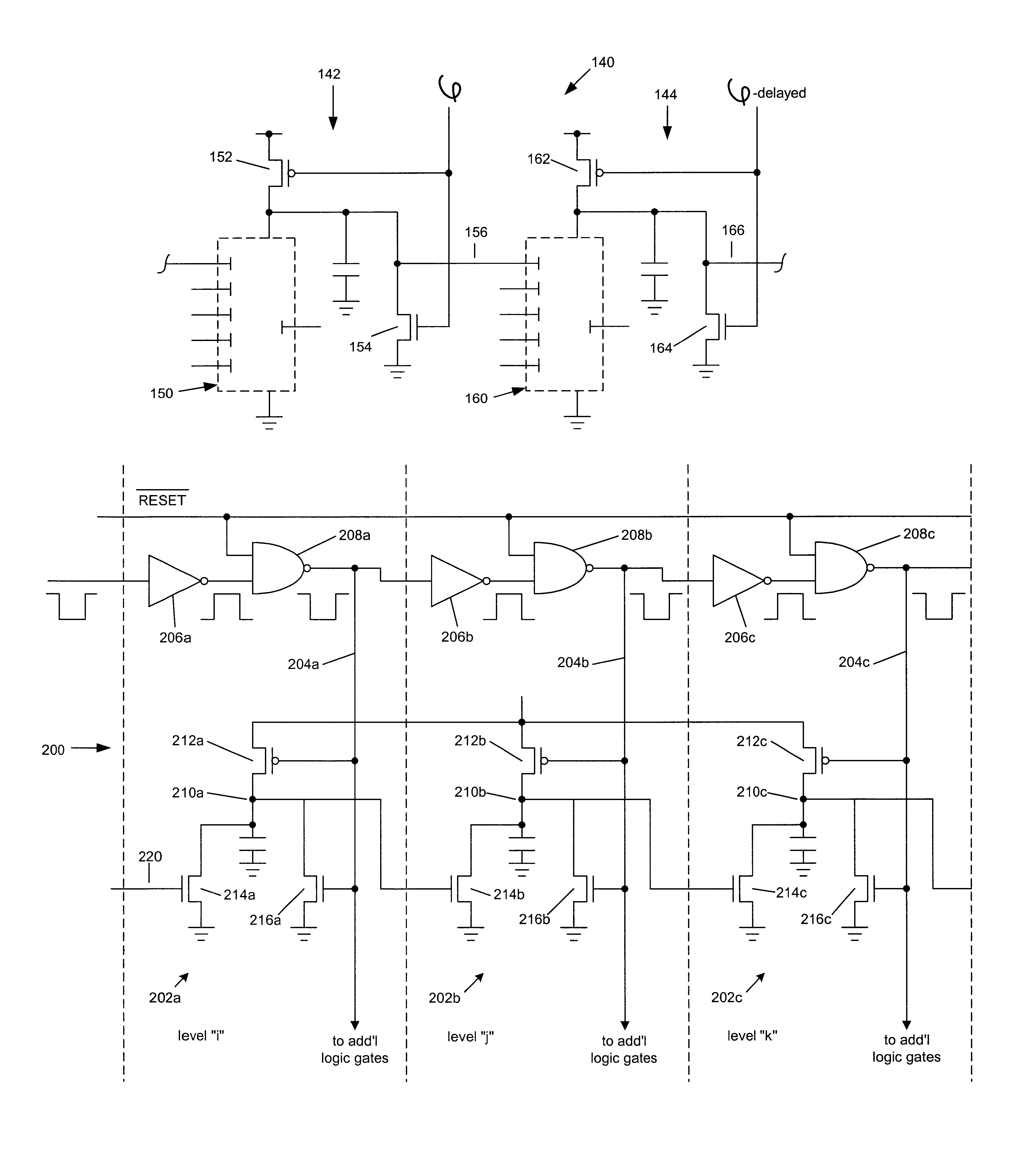
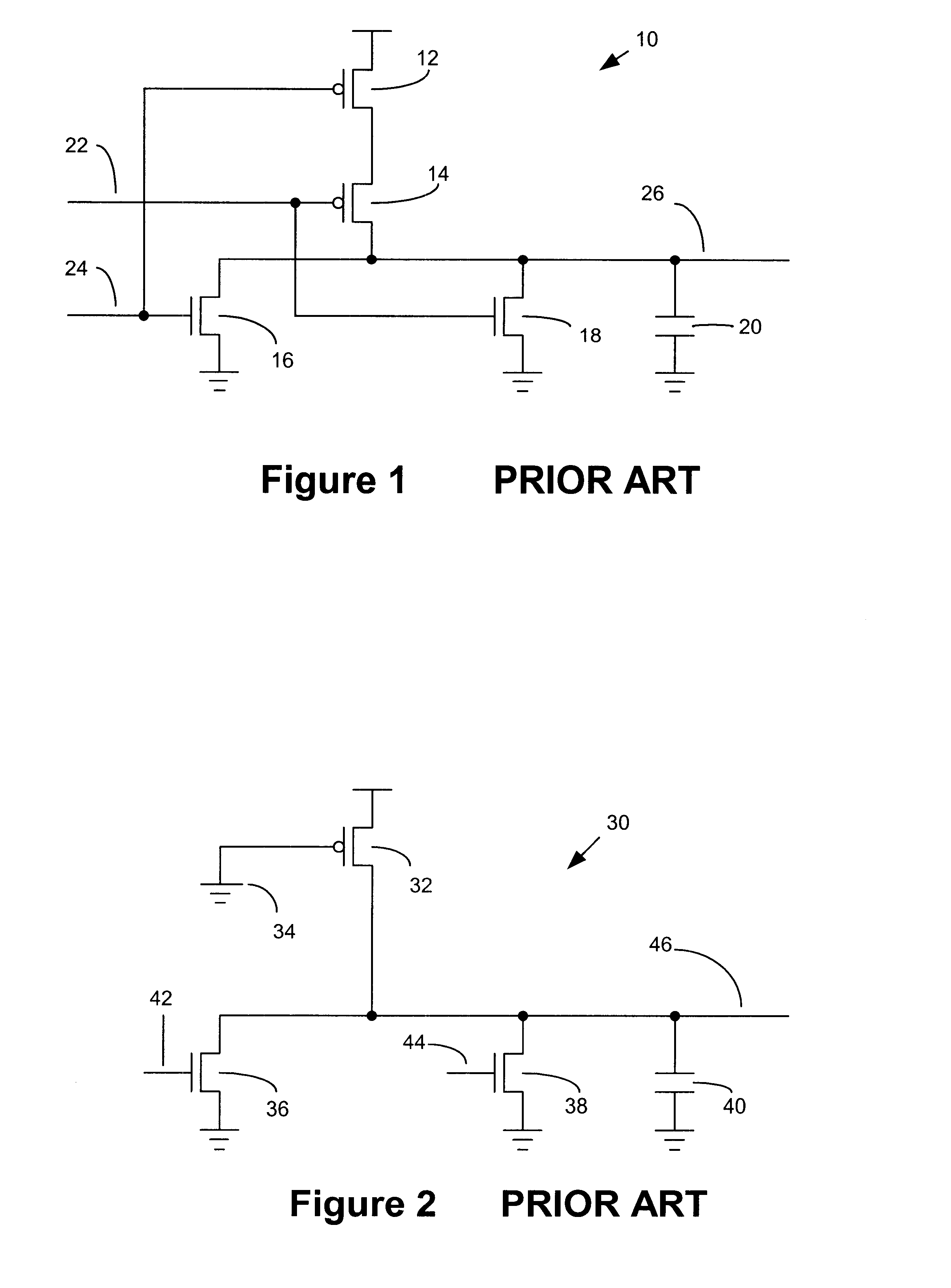
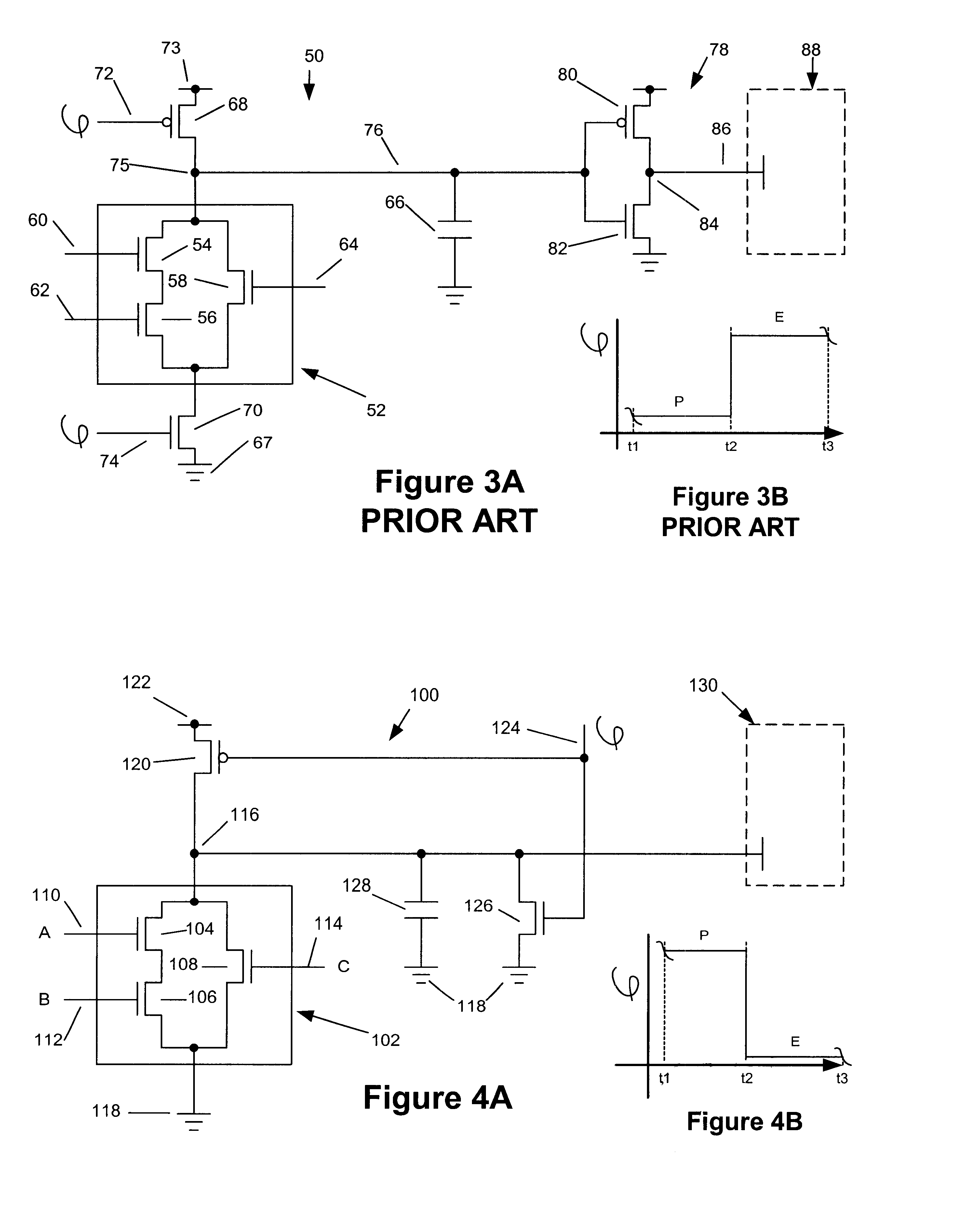
Illustrative embodiments of the invention are described below. In the interest of clarity, not all features of an actual implementation are described in this specification. It will of course be appreciated that in the development of any such actual embodiment, numerous implementation-specific decisions must be made to achieve the developers' specific goals, including, for example, compliance with system-related and business-related constraints, which will vary from one implementation to another. Moreover, it will be appreciated that such a development effort might be complex and time-consuming, but would nevertheless be a routine undertaking for those of ordinary skill in the art having the benefit of this disclosure.

The present invention will now be described with reference to FIGS. 4-6. As will be readily apparent to those skilled in the art upon a complete reading of the present application, the present method is applicable to a variety of technologies, e.g., NMOS, PMOS, CMOS, et...


PUM


Abstract

A logic gate includes a logic circuit having an input node and an output node, an enabling transistor coupled between a first power supply node and the output node, the enabling transistor adapted to couple the output node to the first power supply node during an evaluation phase in the logic gate, and a pre-charge transistor coupled between the output node and a second power supply node, the pre-charge transistor adapted to couple the output node to the second power supply node during a pre-charge phase in the logic gate.

Description

1. Field of the InventionThe present invention relates generally to semiconductor logic devices, and, more particularly, to clocked static logic useful for high frequency operations.2. Description of the Related ArtIntegrated circuitry to implement various logic functions is well known in the semiconductor industry. The use of transistors, capacitors and other integrated circuit elements to implement AND, OR, NAND, NOR, NOT, and other logical operations is well known in that art, and logic circuitry itself has taken on many forms. For example, logic circuitry has been implemented in NMOS technologies as well as in CMOS technologies, each with its own advantages and disadvantages. Moreover, logic circuitry may be implemented in dynamic or static, clocked or not clocked, circuitry. CMOS logic is preferred in many applications because of its relatively low power dissipation, as compared to, for example, NMOS logic.FIG. 1 shows a standard two-input CMOS static logic NOR gate 10, while F...

Claims


Application Information

Patent Timeline
IPC IPC(8): H03K19/096
CPCH03K19/0963
Inventor FORBES, LEONARD
Owner NAN YA TECH
Why Eureka
Try Eureka