Leadless image sensor package structure and method for making the same

Inactive Publication Date: 2002-05-07
SILICONWARE PRECISION IND CO LTD
View PDF8 Cites 494 Cited by
  • Summary
  • Abstract
  • Description
  • Claims
  • Application Information

AI Technical Summary

Problems solved by technology

But because of their relatively good size, they are not adequate for the trend of high integration in the near future.
Although the ceramic carrier having feature of relatively good in sealing can prolong the service life of the image device, it can't meet the demand i

Method used


Image

  • Leadless image sensor package structure and method for making the same
  • Leadless image sensor package structure and method for making the same
  • Leadless image sensor package structure and method for making the same

Examples


Embodiment Construction

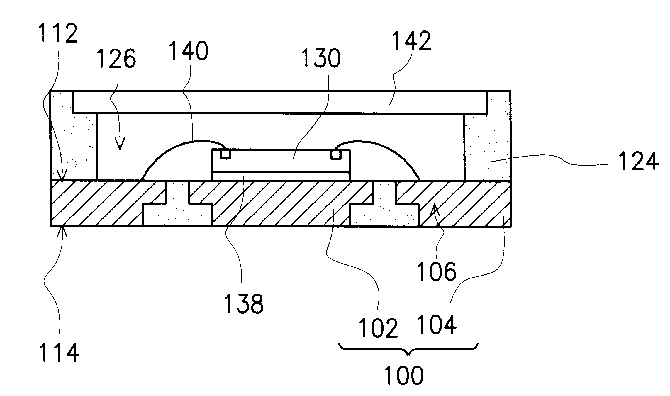
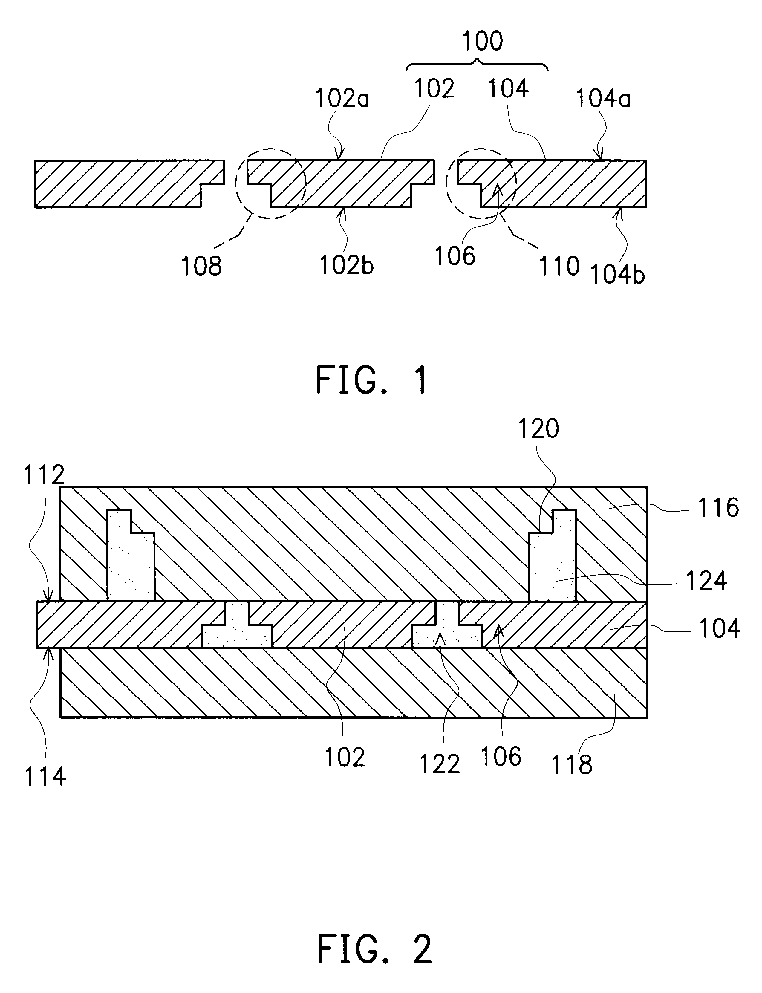
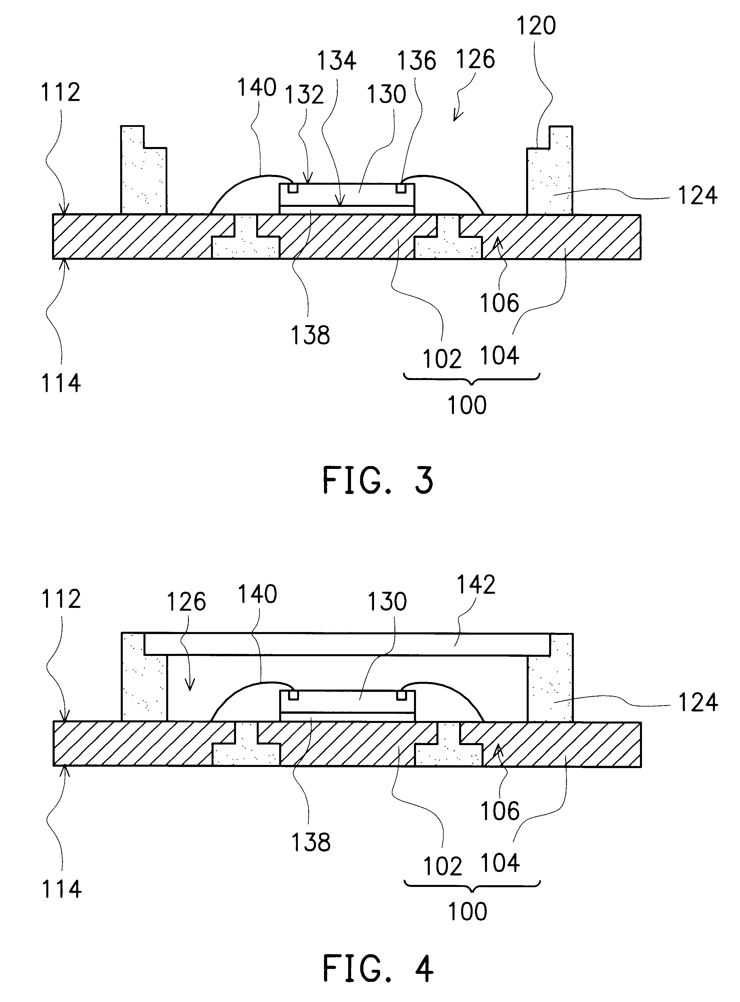
FIG. 1 through FIG. 5 are cross-sectional views of a manufacturing process of a leadless image sensor package structure according to the invention. The leadless image sensor package structure of the invention is constructed on a lead frame 100 that includes a die pad 102 and a plurality of leads 104 disposed at the periphery of the die pad 102 and surrounding thereof. In this embodiment, the die pad 102 has a top surface 102a larger than its bottom surface 102b and a top surface 104a of the lead 104 is also larger than its bottom surface 104b. Therefore, a step-like structure 108 or 110 is formed at the periphery of the die pad 102 and at the wire-bonding portion 106 of the leads 104. The step-like structures 108 and 110 are formed by a "half etching method" or a "coining method" so that the thickness of a portion of the step-like structure 108, 110 can be reduced. The step-like structure s 108 and 110 are used to improve bondability between the lead frame 100 and a below-mentioned ...


PUM


Abstract

A leadless image sensor package constructed on a lead frame includes a die pad and a plurality of leads disposed at the periphery of the die pad. A molding compound, disposed on the top surface of the lead frame and being surrounding the die pad on the periphery of the lead frame, fills the clearance between the die pad and the leads and exposes, on the top surface, the die pad and the wire-bonding portion of the leads. Moreover, the lead frame and the molding compound constitute a "chip containing space" with chip set therein. Further, the chip with its back surface attached to the top surface of the die pad makes use of the wires to electrically connect to the bonding pad and the top surface of the wire-bonding portion, thereafter, a transparent lid is used to cap and seal the "chip containing space".

Description

1. Field of the InventionThis invention relates to an image sensor package structure and method for making the same, and more particularly to a leadless image sensor package structure and method for making the same.2. Description of Related ArtAs the development of multimedia is flourishing recently, the use of digital image has been more and more frequent, consequently, the corresponding requirements for image process devices are increasing. Many digital image products used nowadays including video camera, PC digital video camera, and even optical scanner and visual telephone etc. acquire images by the use of image sensor. The image sensor including Charge Coupled Device (CCD) and Complementary Metal-Oxide Semiconductor (CMOS) sensor etc. can sensitively receive light beam transmitted by the image and convert into digital signal. Since image sensor needs to receive light source, its package type is quite different from that of any common electronic product.Conventional image sensor...

Claims


Application Information

Patent Timeline
IPC IPC(8): H01L21/02H01L23/48H01L23/055H01L21/50H01L23/498H01L23/02
CPCH01L21/50H01L23/49861H01L24/97H01L27/14618H01L23/055H01L2224/32245H01L2224/48247H01L2224/92H01L2224/92247H01L2224/97H01L2924/01009H01L2924/01078H01L2924/01082H01L2924/16195H01L2924/01087H01L2924/01033H01L24/48H01L2224/73265H01L2224/48091H01L2224/83H01L2224/85H01L2924/00014H01L2924/00012H01L24/73H01L2224/05599H01L2224/45099H01L2224/85399H01L2924/181H01L2924/351H01L2924/00H01L2224/45015H01L2924/207
Inventor HUANG, CHIEN-PING
Owner SILICONWARE PRECISION IND CO LTD
Why Eureka
Try Eureka