Micro-electro-mechanical optical device

Inactive Publication Date: 2002-05-21
LUCENT TECH INC +1
View PDF6 Cites 25 Cited by
  • Summary
  • Abstract
  • Description
  • Claims
  • Application Information

AI Technical Summary

Problems solved by technology

Such micro-electro-mechanical structures provide a limited range of motion for optical devices coupled thereto which makes them undesirable.

Method used


Image

  • Micro-electro-mechanical optical device
  • Micro-electro-mechanical optical device
  • Micro-electro-mechanical optical device

Examples


Embodiment Construction

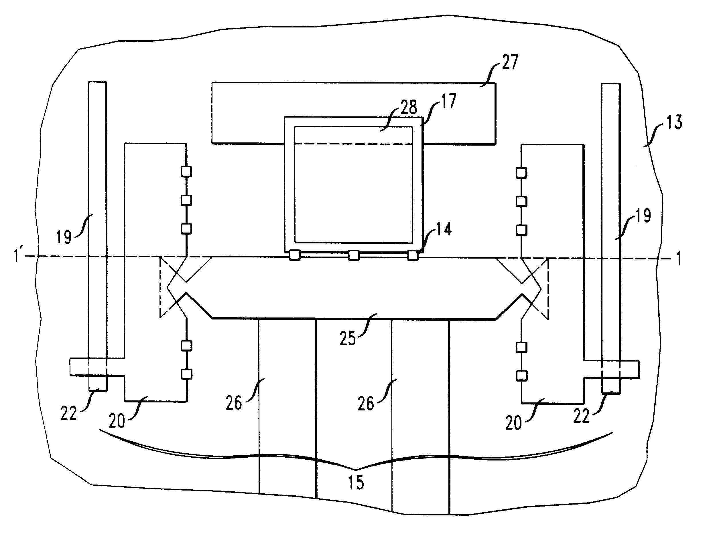
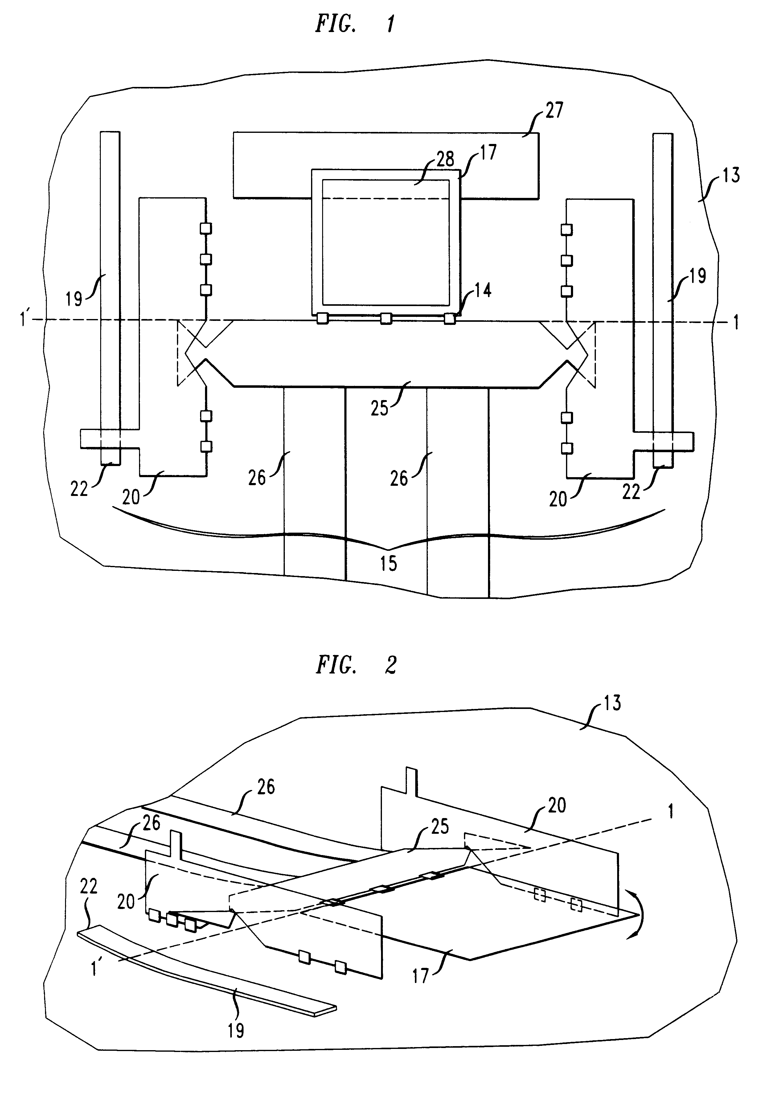
A micro-electro-mechanical optical device having the structure depicted in FIG. 1 was obtained from the MEMS Technology Application Center, MCNC, Research Triangle Park, N.C. The micro-electro-mechanical optical device was disposed on a surface of a silicon substrate. The silicon substrate had a resistivity of about 1-2 ohm-cm. A multi-layered planar arrangement of alternating polysilicon layers (POLY0, POLY1 and POLY2) and phosphosilicon glass layers (OX1 and OX2), formed over a 600 nm (nanometer) thick silicon nitride layer was formed on the silicon substrate.

The polysilicon layers POLY0, POLY1 and POLY2 had thicknesses of about 0.5 .mu.m (micrometers), 2.0 .mu.m, and 1.5 .mu.m, respectively. The phosphosilicon glass layers OX1 and OX2 had thicknesses of about 2 .mu.m and 0.75 .mu.m, respectively. A 0.5 .mu.m layer of Cr / Au was formed on the POLY2 layer.

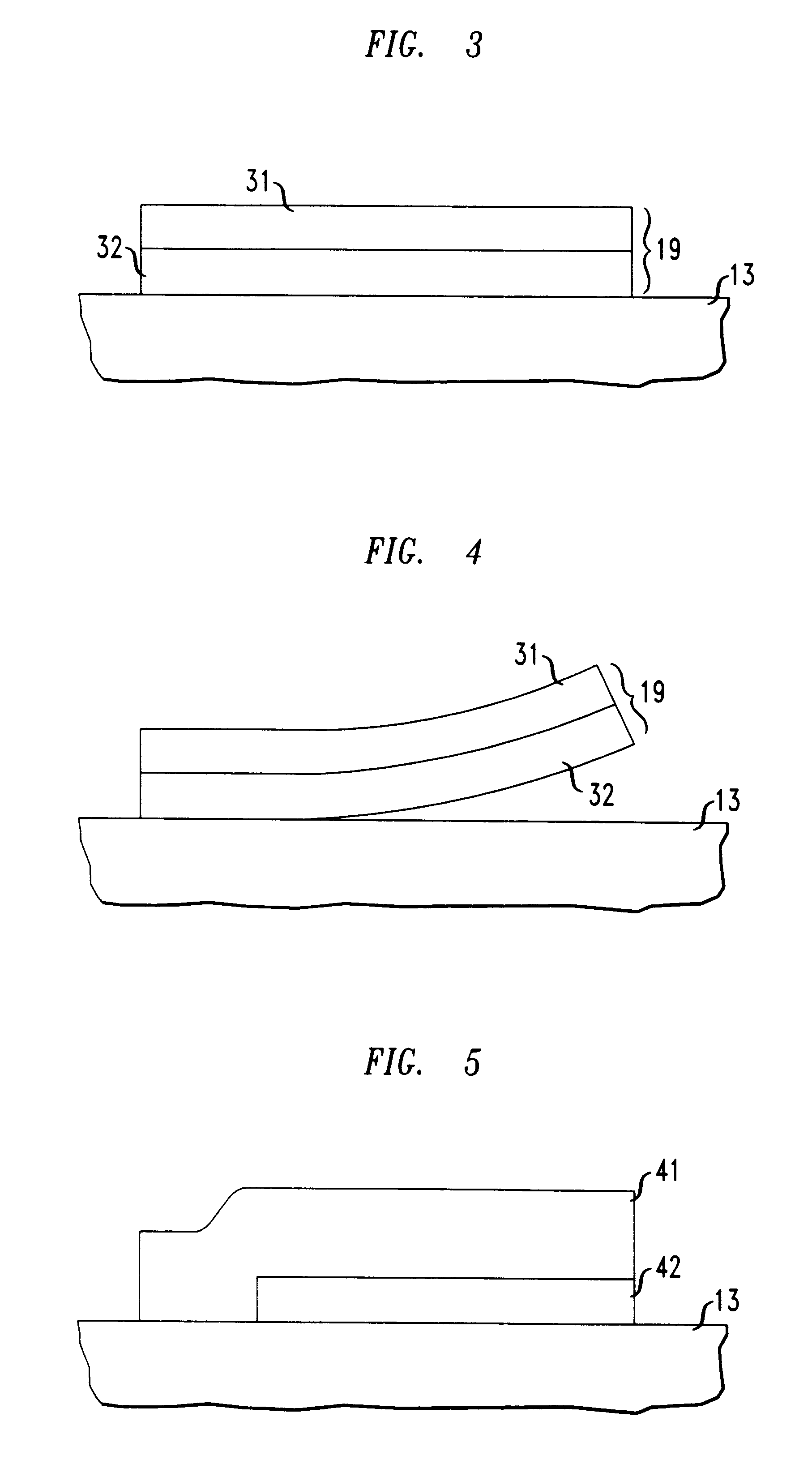
The silicon nitride layer, the polysilicon layers (POLY0, POLY1 and POLY2), the phosphosilicon glass layers (OX1 and OX2), and th...


PUM


Abstract

A micro-electro-mechanical optical device is disclosed. The micro-electro-mechanical optical device includes a micro-electro-mechanical structure coupled with an optical device. Both the micro-electro-mechanical structure and the optical device are disposed on a substrate surface. The micro-electro-mechanical structure lifts the optical device a predetermined distance above the plane of the substrate surface. Thereafter, the lifted optical device is moveable relative to the plane of the substrate surface in response to an electrostatic field generated between the optical device and the substrate.

Description

The present invention relates generally to optical communication systems and more particularly, to micro-electro-mechanical optical devices.DESCRIPTION OF THE RELATED ARTOptical communication systems typically include a variety of optical devices (e.g., light sources, photodetectors, switches, attenuators, mirrors, amplifiers, and filters). The optical devices transmit, modify, or detect optical signals in the optical communications systems. Some optical devices are coupled to micro-electro-mechanical structures (e.g., thermal actuators) forming a micro-electro-mechanical optical device. The term micro-electro-mechanical structure as used in this disclosure refers to a microscopic structure that moves mechanically under the control of an electrical signal.Cowan, William D., et al., "Vertical Thermal Actuators for Micro-Opto-Electro-Mechanical Systems", SPIE, Vol. 3226, pp. 137-146 (1997), describes a micro-electro-mechanical structure useful for moving optical devices. In Cowan et a...

Claims


Application Information

Patent Timeline
Patent Type & Authority Patents(United States)
IPC IPC(8): B81B3/00G02B26/08F16S1/02B81B5/00B81B7/00
CPCB81B3/004B81B3/0062B81B5/00G02B26/0866G02B26/0841B81B7/0003B81B2201/042B81B2201/045
Inventor AKSYUK, VLADIMIR ANATOLYEVICHBISHOP, DAVID JOHN
Owner LUCENT TECH INC
Why Eureka
Try Eureka