

Active matrix LCD in which a change in the storage capacitance Cs due to having multiple exposure regions is compensated for by a change in the coupling capacitance Cgd
a liquid crystal display and active matrix technology, applied in non-linear optics, identification means, instruments, etc., can solve problems such as deteriorating display quality, deteriorating display quality, and deteriorating display quality
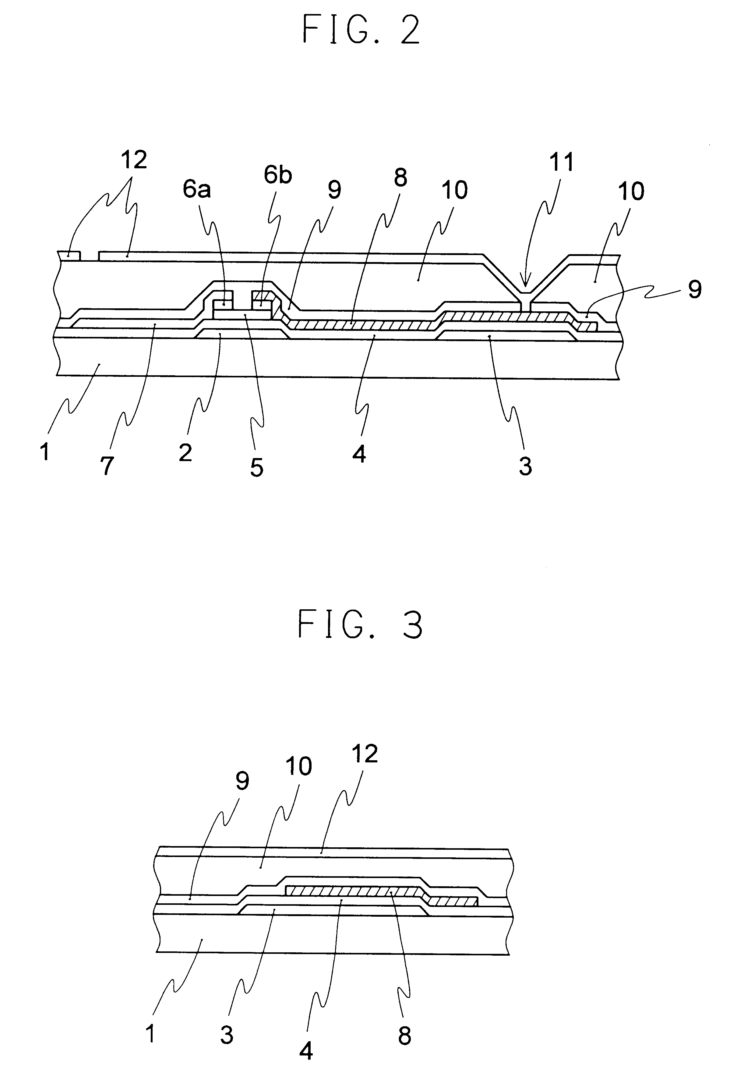
- Summary
- Abstract
- Description
- Claims
- Application Information
AI Technical Summary
Problems solved by technology
Method used
Image

Examples
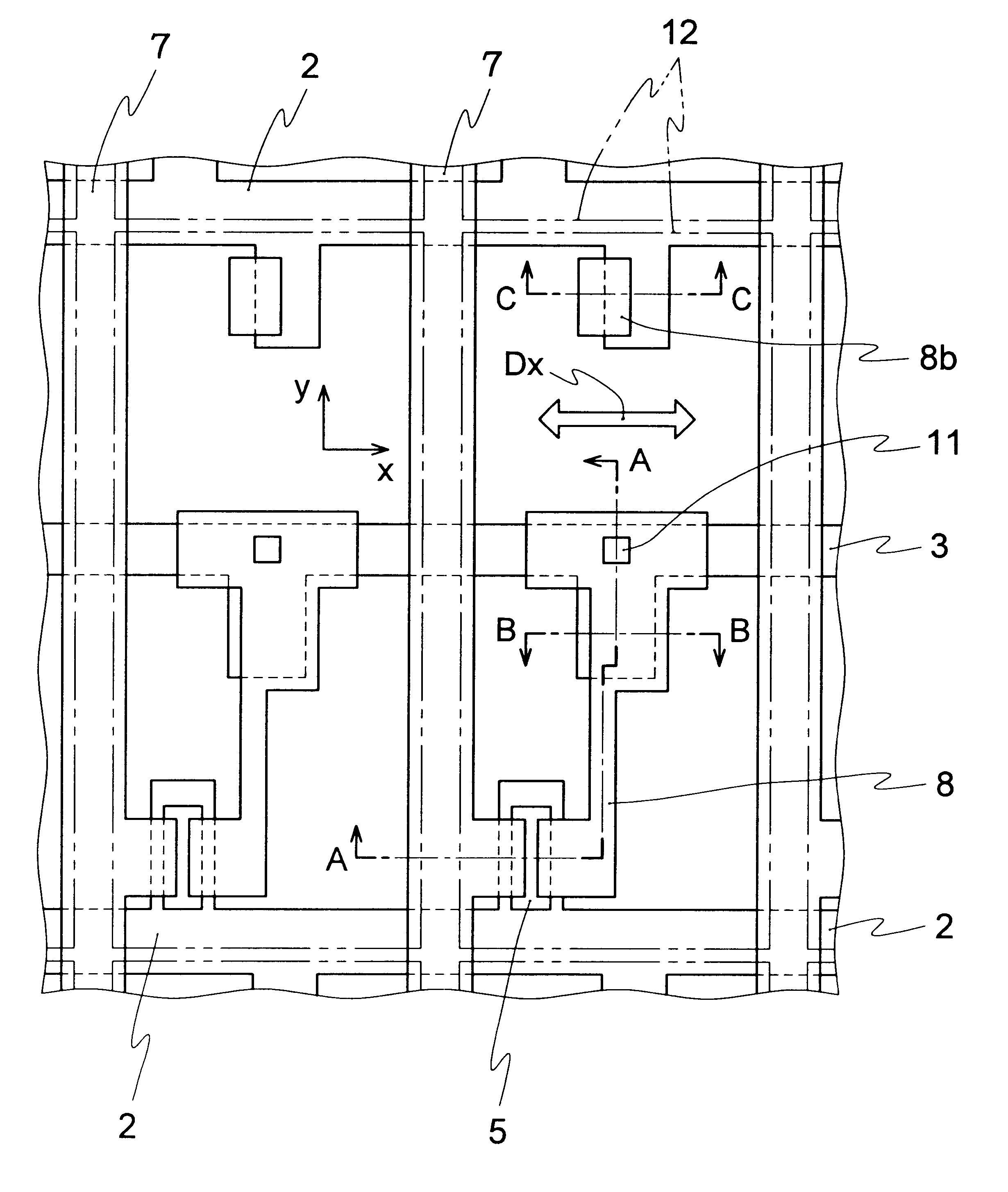
embodiment 1
In EMBODIMENT 1 provided as described, as storage capacitance is formed to compensate for the change of the Cgd for each exposing region, the .DELTA.Vgd value becomes constant even if the exposing region is different, and the displaying quality reduction such as flickering, image sticking and nonuniform displaying can be prevented. Thus, a liquid crystal displaying apparatus can be provided which is high in displaying quality and is easy to manufacture and high in yield.
embodiment 2
FIG. 6 is a plan view of one portion of the pixel of EMBODIMENT 2 of the present invention. FIG. 7 is a sectional illustrating view taken along a line of A--A of FIG. 6. FIG. 8 is a sectional illustrating view taken along a line of B--B of FIG. 6. In EMBODIMENT 1, the drain electrode 8 is extended so far as a portion for directly forming the storage capacitance. In this embodiment, the drain electrode 8 is separated from an electrode 8a for forming the storage capacitance, and EMBODIMENT 2 is the same as EMBODIMENT 1 in the other respects. The drain electrode 8 and an electrode 8a for forming the storage capacitance are electrically connected through a pixel electrode 12 by a contact hole 13 for electrically connecting the drain electrode 8 and the pixel electrode 12, and a contact hole 11 for electrically connecting the pixel electrode 12 and an electrode 8a for forming the storage capacitance. Even in this configuration, the same effects as those of EMBODIMENT 1 are obtained. In E...
embodiment 3
FIG. 9 is a plan illustration view of one portion of the pixel of EMBODIMENT 3 of the present invention. FIG. 10 is a section al illustrating view taken along a line A--A of FIG. 9. FIG. 11 is a sectional illustrating view taken along a line of B--B of FIG. 9. In EMBODIMENT 1, the TFT connects with the scanning wiring 2 by an electrode and is formed on it. In EMBODIMENT 3, the TFT is formed on the scanning wiring 2, and in other respects, EMBODIMENT 3 is the same as EMBODIMENT 1. In EMBODIMENT 3, in the Cgd, the drain electrode 8 is deviated to an arrow direction of FIG. 9, namely, in FIG. 9, to the axial direction in position, whereby the value is changed. It is necessary to change a direction of changing the storage capacitance Cs value to the y axial direction. In EMBODIMENT 3, when the drain electrode 8 is relatively deviated to the--y direction with respect to the scanning wiring 2, the superposing area between the drain electrode 8 and the scanning wiring 2 increases to increa...
PUM
| Property | Measurement | Unit |
|---|---|---|
| storage capacitance | aaaaa | aaaaa |
| coupling capacitance | aaaaa | aaaaa |
| transparent | aaaaa | aaaaa |
Abstract
Description
Claims
Application Information