
Method and apparatus for optimal wafer-by-wafer processing

a technology of wafer-by-wafer processing and automatic error correction, applied in the direction of instrumentation, total factory control, programme control, etc., can solve the problems of only updating a few exposure tool settings, adversely affecting process steps, and non-uniform quality of semiconductor devices

Inactive Publication Date: 2002-07-30
GLOBALFOUNDRIES INC
View PDF8 Cites 68 Cited by
  • Summary
  • Abstract
  • Description
  • Claims
  • Application Information

AI Technical Summary

Problems solved by technology

One of the process steps that are adversely affected by such factors is the photolithography overlay process.
Some of the problems associated with the current methods include the fact that the exposure tool settings are only updated a few times a month.
Furthermore, wafer-to-wafer manufacturing variations can cause non-uniform quality of semiconductor devices.

Method used


Image

  • Method and apparatus for optimal wafer-by-wafer processing
  • Method and apparatus for optimal wafer-by-wafer processing
  • Method and apparatus for optimal wafer-by-wafer processing

Examples


Embodiment Construction

Illustrative embodiments of the invention are described below. In the interest of clarity, not all features of an actual implementation are described in this specification. It will of course be appreciated that in the development of any such actual embodiment, numerous implementation-specific decisions must be made to achieve the developers' specific goals, such as compliance with system-related and business-related constraints, which will vary from one implementation to another. Moreover, it will be appreciated that such a development effort might be complex and time-consuming, but would nevertheless be a routine undertaking for those of ordinary skill in the art having the benefit of this disclosure.

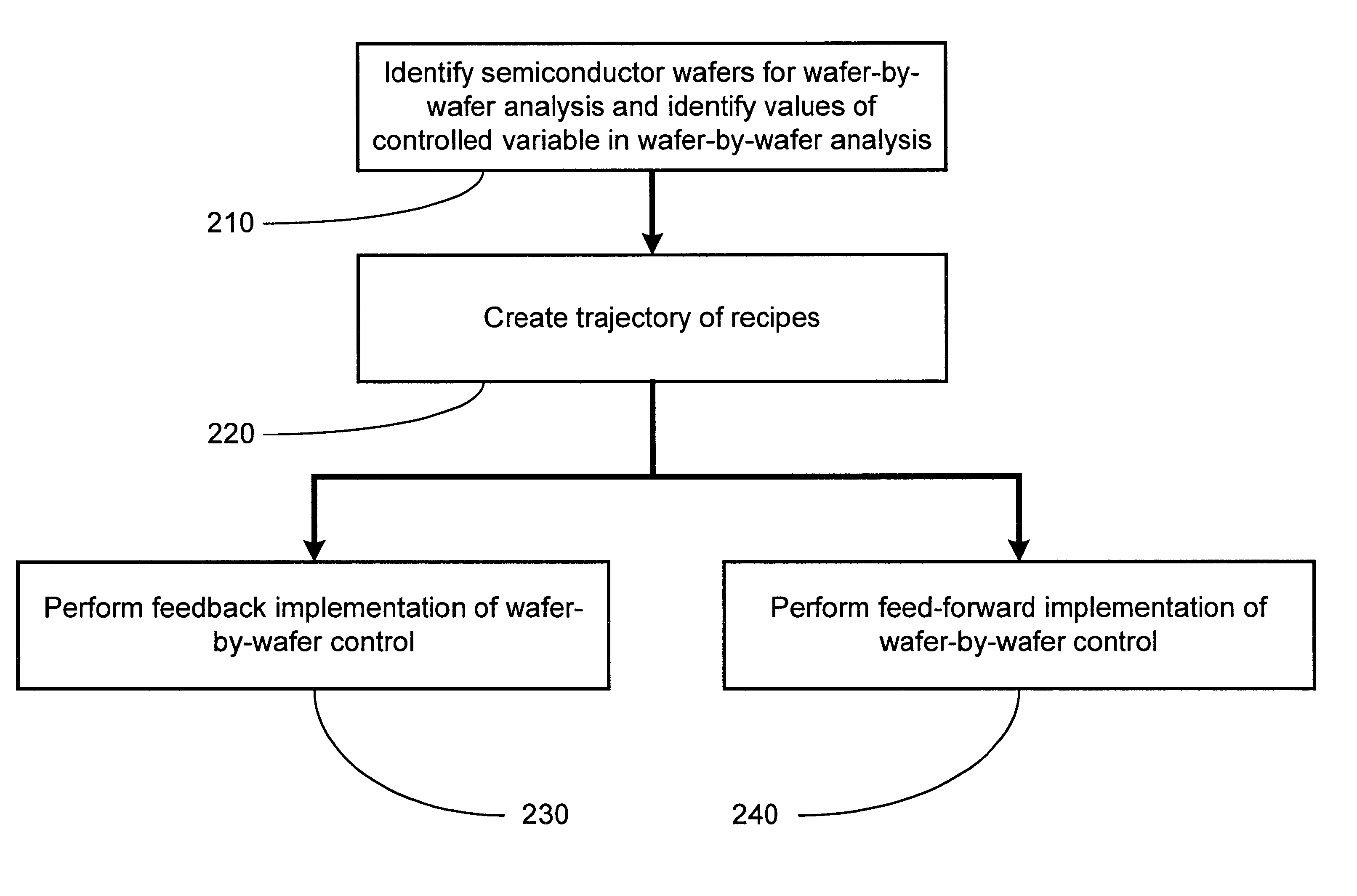
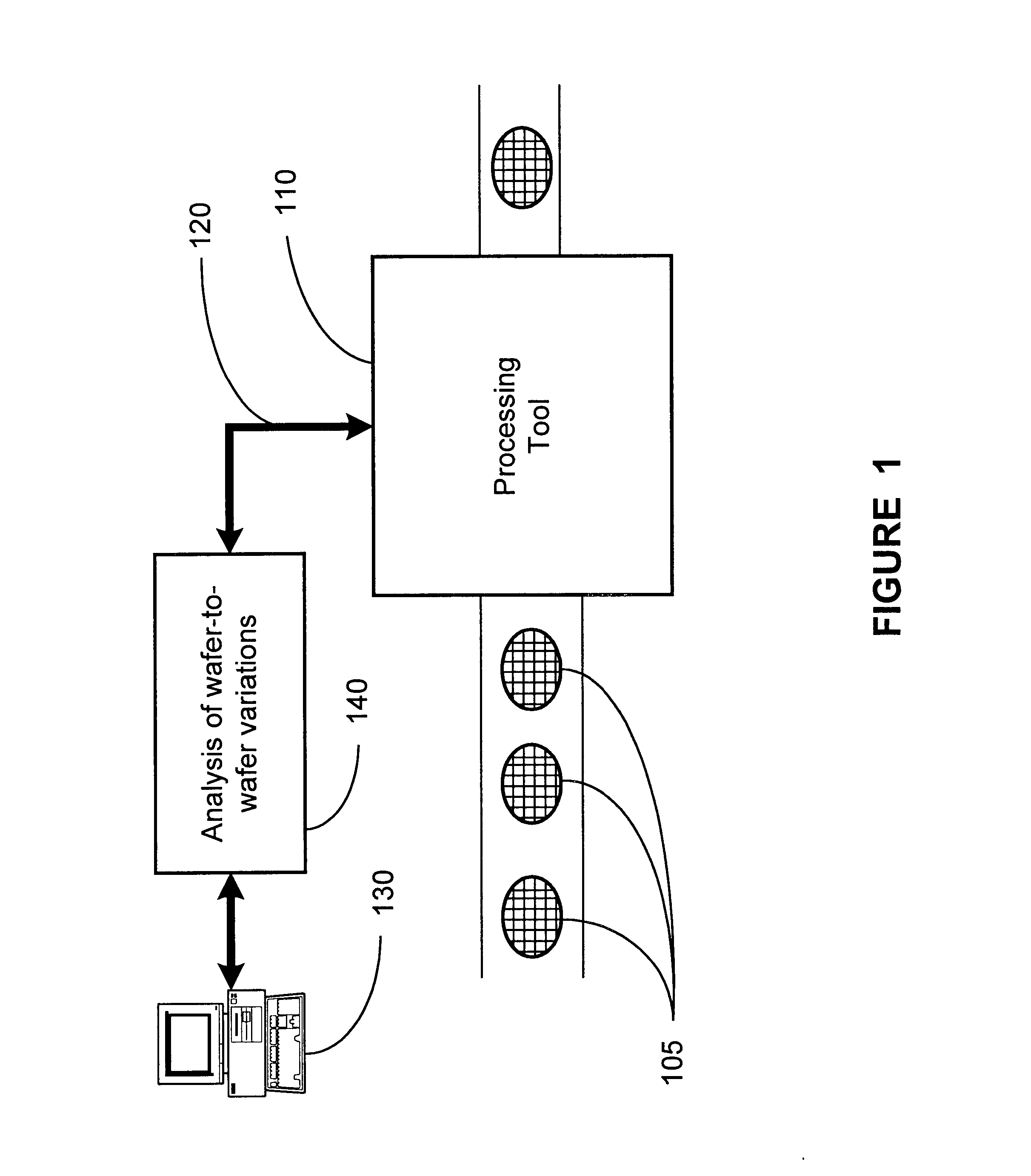
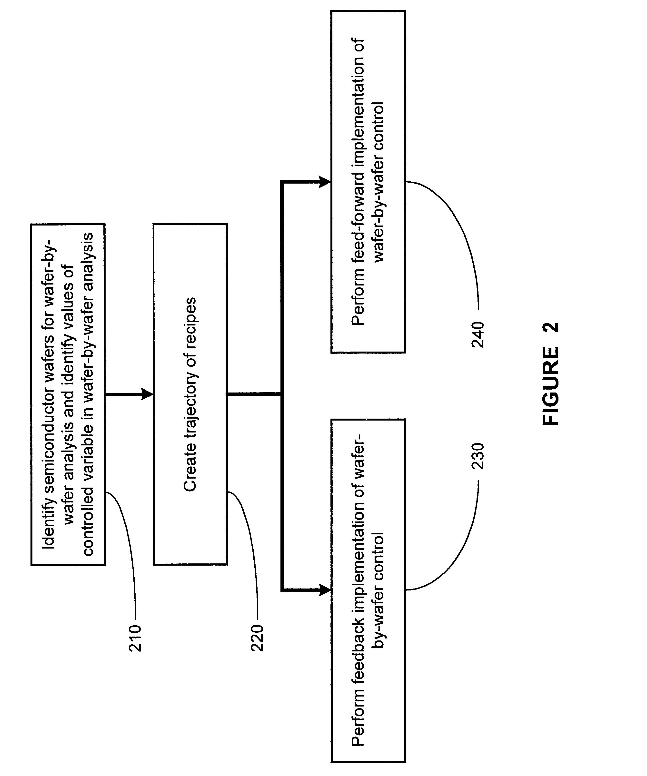
There are many discreet processes that are involved in semiconductor manufacturing. Many times, semiconductor devices are stepped through multiple manufacturing process tools. Wafer-to-wafer variations can result in an output of non-uniform semiconductor devices. One process that is af...


PUM


Abstract

The present invention provides for a method and an apparatus for optimal wafer-by-wafer processing. Semiconductor devices are identified for wafer-by-wafer analysis. At least one value of a controlled variable in the wafer-by-wafer analysis is identified. A trajectory of recipes is created for the identified semiconductor devices. A feedback implementation of wafer-by-wafer control is performed using the trajectory of recipes upon the identified semiconductor devices. A feed-forward implementation of wafer-by-wafer control is performed using the trajectory of recipes upon the identified semiconductor devices.

Description

1. Field of the InventionThis invention relates generally to semiconductor products manufacturing, and, more particularly, to a method and means for automated error correction for wafer-by-wafer processing.2. Description of the Related ArtThe technology explosion in the manufacturing industry has resulted in many new and innovative manufacturing processes. Today's manufacturing processes, particularly semiconductor manufacturing processes, call for a large number of important steps. These process steps are usually vital, and therefore, require a number of inputs that are generally fine tuned to maintain proper manufacturing control.The manufacture of semiconductor devices requires a number of discrete process steps to create a packaged semiconductor device from raw semiconductor material. The various processes, from the initial growth of the semiconductor material, the slicing of the semiconductor crystal into individual wafers, the fabrication stages (etching, doping, ion implantin...

Claims


Application Information

Patent Timeline
IPC IPC(8): G05B19/418G06Q10/00H01L21/00G06Q10/06
CPCG05B19/41865G06Q10/06H01L21/67276G05B2219/32077G05B2219/45031Y02P90/02
Inventor TOPRAC, ANTHONY J.
Owner GLOBALFOUNDRIES INC
Features
  • Generate Ideas
  • Intellectual Property
  • Life Sciences
  • Materials
  • Tech Scout
  • Unparalleled Data Quality
  • Higher Quality Content
  • 60% Fewer Hallucinations
Learn More