Process and system for maintaining 3 sigma process tolerance for parasitic extraction with on-the-fly biasing

a process tolerance and parasitic extraction technology, applied in the field of process and system for maintaining a 3 sigma process tolerance for parasitic extraction with on-the-fly biasing, can solve the problems of limiting the designer's ability to efficiently utilize the size of devices and wiring within the integrated circuit design, and conventional methods are not allowed

Inactive Publication Date: 2002-08-06
IBM CORP
View PDF1 Cites 36 Cited by
  • Summary
  • Abstract
  • Description
  • Claims
  • Application Information

AI Technical Summary

Problems solved by technology

However, conventional systems suffer from the drawback that only the theoretical maximum and minimum variances within the manufacturing process are considered when performing integrated circuit design.
Therefore, conventional systems are designed for potentially unrealistic parasitic values, which limits the designer's ability to efficiently utilize the size of devices and wiring within the integrated circuit design.
Conventional methods do not allow this.
Overlay variations cause two or more levels to be shifted towards each other, which destroy the symmetry in symmetrically laid out devices.
This lack of symmetry impacts stability in storage cells and other circuits which rely on equal devices.

Method used


Image

  • Process and system for maintaining 3 sigma process tolerance for parasitic extraction with on-the-fly biasing
  • Process and system for maintaining 3 sigma process tolerance for parasitic extraction with on-the-fly biasing
  • Process and system for maintaining 3 sigma process tolerance for parasitic extraction with on-the-fly biasing

Examples


Embodiment Construction

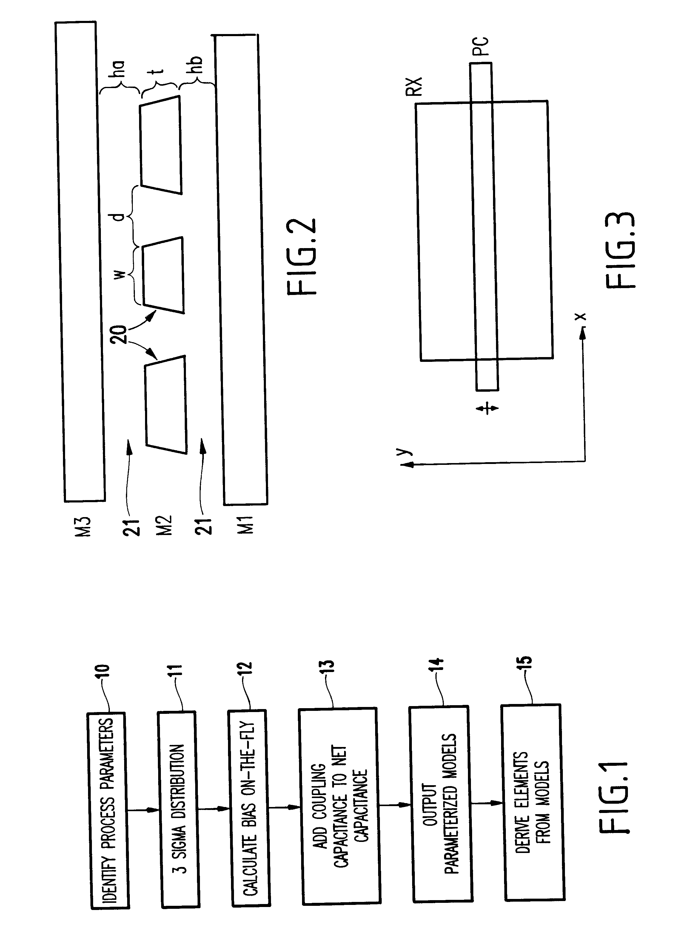
Typically, parasitic capacitance and resistance values of an integrated circuit are determined by the geometry, resistivity, via resistance and dielectric properties. For each main independent process parameter that influences the process parameters, a nominal value and distribution is determined, measured and controlled during manufacturing. Furthermore, the manufacturing process is not exactly reproducible and the value of each process parameter is more accurately modeled by a distribution function, taking into account the variability of the lateral biases, vertical dimensions and material properties. The distribution function is assumed to be the shape of a Gaussian function. The width of this function is expressed in units of sigma, so that 99.73% of all possible values are within a 3 sigma limit.

Key values of the extracted parasitics are coupling capacitances, load capacitances, and wire RC delays. With the invention, the sensitivity of these values to the independent process p...


PUM


Abstract

A method and structure for a method of determining characteristics of parasitic elements in an integrated circuit comprising, identifying manufacturing process parameters of devices in the integrated circuit, calculating a parasitic performance distribution for each of the devices based on the manufacturing process parameters, combining the parasitic performance distribution for each of the devices into a net parasitic value, and forming a parameterized model based on the net parasitic values.

Description

1. Field of the InventionThe present invention generally relates to identifying parasitic values of devices / networks making up integrated circuits and more particularly to a process and system for maintaining a 3 sigma process tolerance for parasitic extraction with on-the-fly biasing.2. Description of the Related ArtWhen integrated circuits are designed, various competing goals must be balanced to achieve a circuit which performs as desired. One such goal is the control of parasitic parameters. For example, coupling capacitances, load capacitances, and wire RC delays are common parasitic parameters. Conventionally, designers prepare a model of an integrated circuit. The model traditionally includes devices such as transistors, capacitors, logic devices, etc. connected by wiring. The parasitic parameters of the devices and the wiring is determined or estimated from previous empirical testing.In addition, the integrated circuit designer must take into account that the manufacturing p...

Claims


Application Information

Patent Timeline
Patent Type & Authority Patents(United States)
IPC IPC(8): G06F17/50
CPCG06F17/5036G06F30/367
Inventor DEWEY, L. WILLIAMHABITZ, PETER A.MCCULLEN, JUDITH H.SEIBERT, EDWARD W.
Owner IBM CORP
Why Eureka
Try Eureka