Programmable chalcogenide fuse within a semiconductor device

a chalcogenide fuse and programmable technology, applied in the direction of solid-state devices, basic electric elements, instruments, etc., can solve the problems of fuses not being reprogrammed, adding delays to manufacturing, and huge reliability problems

Inactive Publication Date: 2002-09-10
OVONYX MEMORY TECH LLC
View PDF10 Cites 116 Cited by
  • Summary
  • Abstract
  • Description
  • Claims
  • Application Information

AI Technical Summary

Problems solved by technology

One drawback of such method is the requirement of additional tools, such as lasers with steppers, and programming algorithms, which adds delays to manufacturing.
Another drawback is that some programmable fuses, such as titanium tung

Method used


Image

  • Programmable chalcogenide fuse within a semiconductor device
  • Programmable chalcogenide fuse within a semiconductor device
  • Programmable chalcogenide fuse within a semiconductor device

Examples


Embodiment Construction

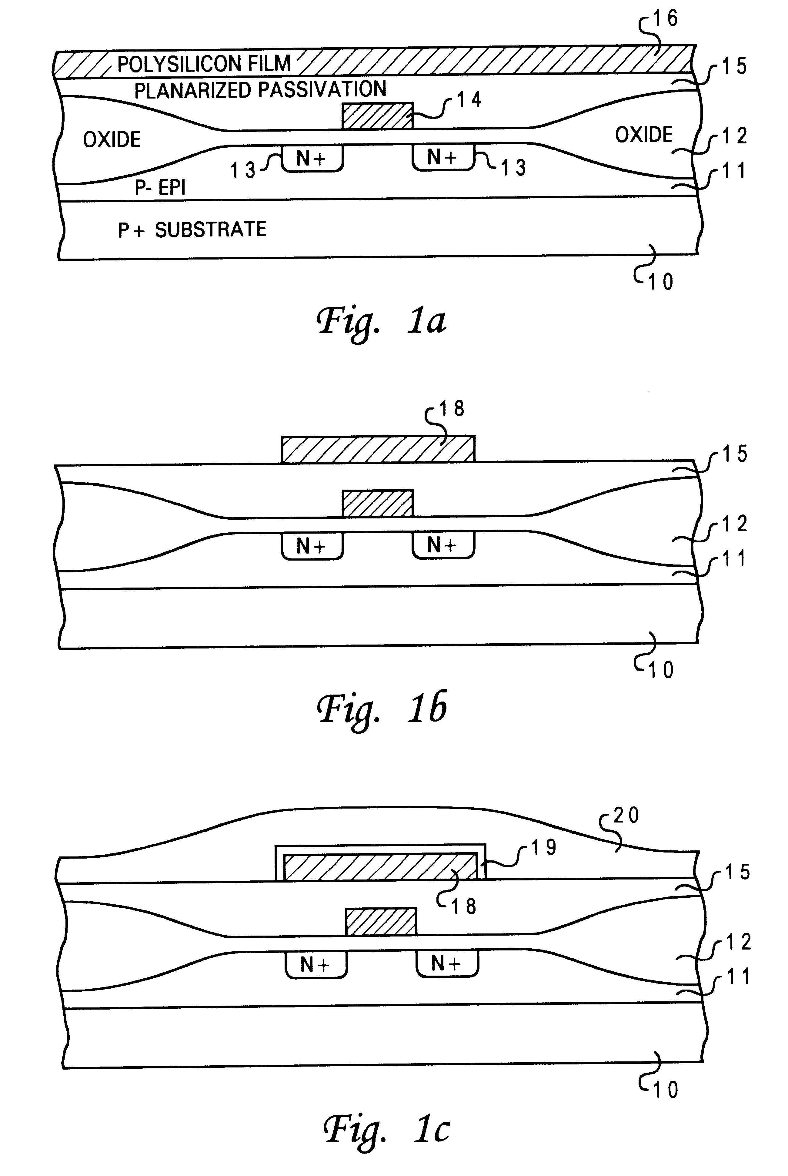
The present invention is illustrated with a complementary-metal-oxide semiconductor (CMOS) processing method, though other types of processing technology may also be applicable.

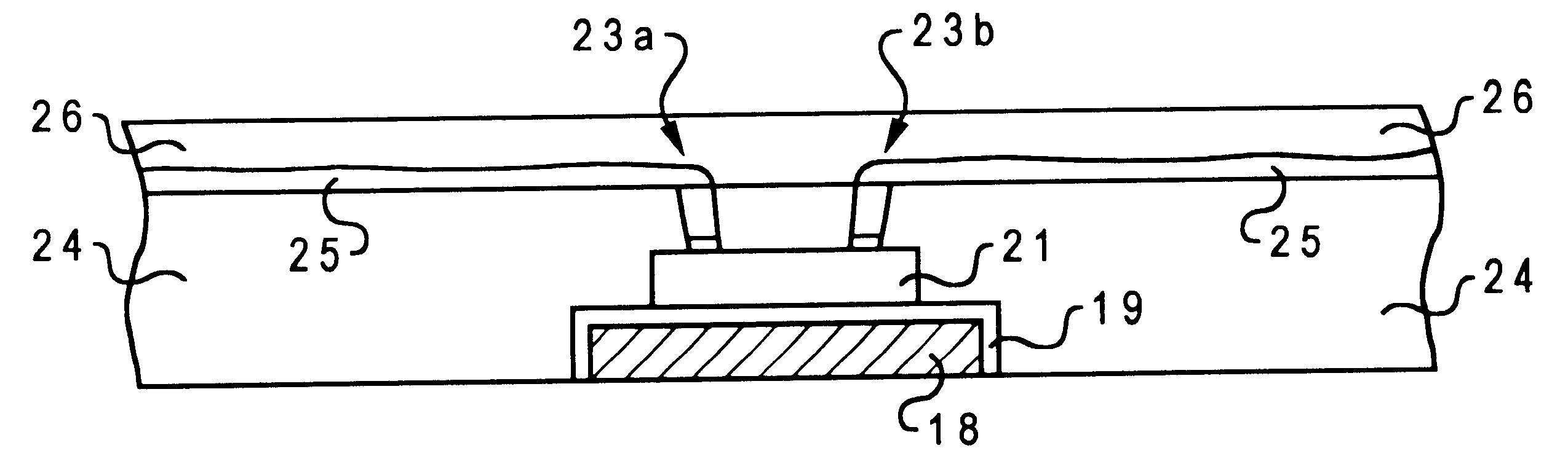
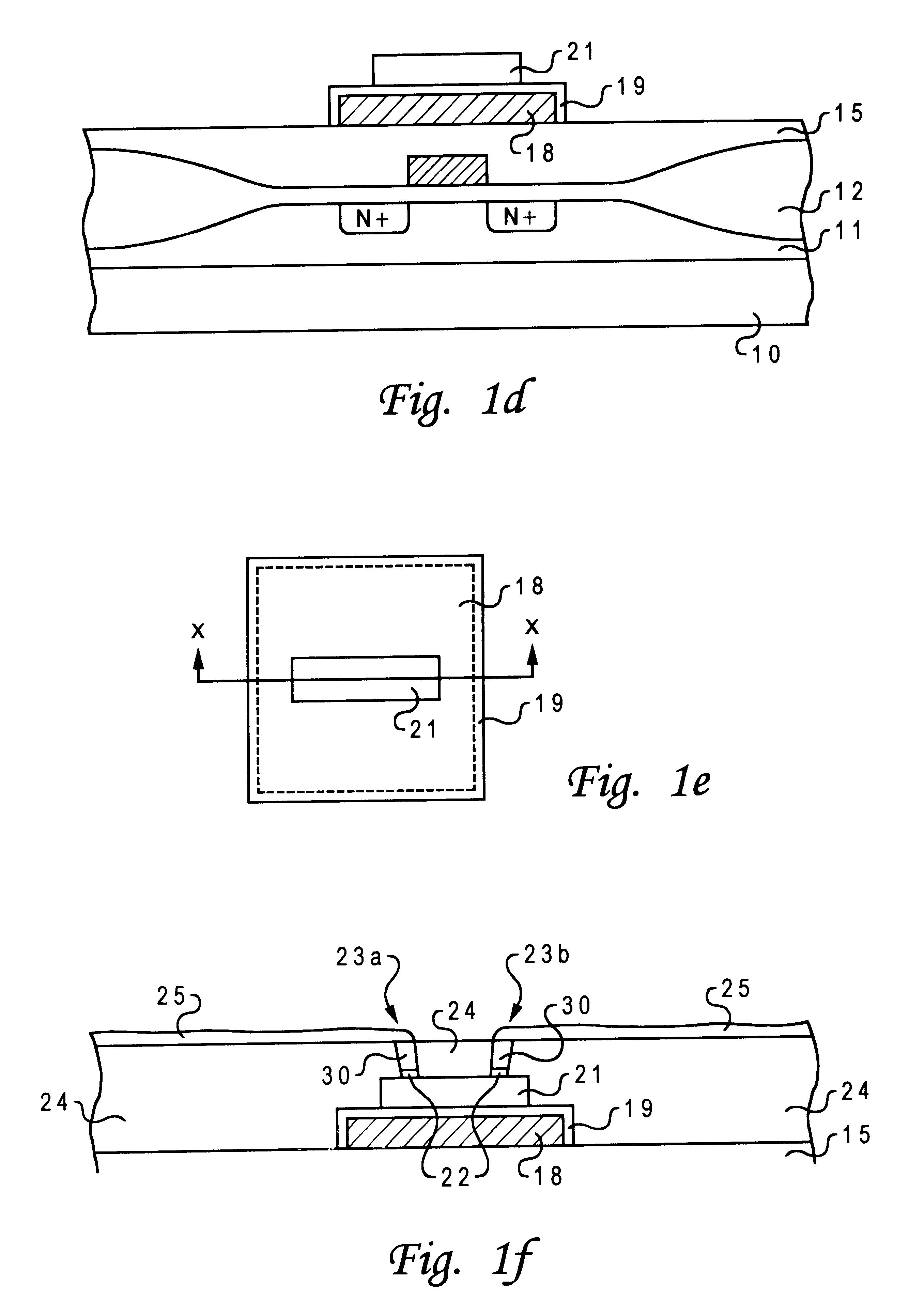
Referring now to the drawings and in particular to FIGS. 1a-1h, there are illustrated pictorial representations of a process for fabricating a programmable chalcogenide fuse within an integrated circuit, in accordance with a preferred embodiment of the present invention. The process begins with a silicon wafer having an optional epitaxial layer on which active devices can be built. As shown in FIG. 1a, a silicon substrate 10 includes an optional epitaxial layer 11. A silicon dioxide (SiO.sub.2) layer 12 having multiple local oxidations of silicon (LOCOS) isolations or shallow trench isolations (STI) may be utilized to isolate one active device from another. In this example, the active device is a transistor formed by n-type diffusions 13 and a polysilicon gate 14. The transistor is covered by a planarized pas...


PUM


Abstract

A method for manufacturing a programmable chalcogenide fuse within a semiconductor device is disclosed. A resistor is initially formed on a substrate. Then, a chalcogenide fuse is formed on top of the resistor. Finally, a conductive layer is deposited on top of the chalcogenide fuse for providing electrical conduction to the chalcogenide fuse.

Description

1. Technical FieldThe present invention relates to a method for manufacturing semiconductor devices in general, and in particular to a method for manufacturing programmable fuses. Still more particularly, the present invention relates to a method for manufacturing a programmable chalcogenide fuse within a semiconductor device.2. Description of the Prior ArtRedundancy circuitry is typically employed to improve the yield of integrated circuits that fail due to localized defects. For example, when a memory cell has a defect that prohibits functionality, a redundant circuit can be switched in via a physical disconnection of a wiring element, commonly known as a fuse, via laser energy. Such programming of redundant circuits is usually performed during the manufacturing process and is hidden from users.Programmable fuses are often utilized to implement redundancy repair on memory devices or to provide lot identification. A commonly used programmable fuse structure in a memory device is co...

Claims


Application Information

Patent Timeline
IPC IPC(8): H01L23/52H01L23/525
CPCH01L23/5256G11C13/0004H01L2924/0002H01L2924/00
Inventor DAVIS, JOHN D.MCINTYRE, THOMAS J.RODGERS, JOHN C.STURCKEN, KEITH K.SPREEN, PETER W.SHAH, TUSHAR K.
Owner OVONYX MEMORY TECH LLC
Why Eureka
Try Eureka