

Plural interleaved exposure process for increased feature aspect ratio in dense arrays
a feature aspect ratio and interleaved technology, applied in the field of semiconductor device manufacturing, can solve the problems of insufficient room to bias the shapes to achieve the desired aspect ratio, inability to overcome the effect of 2 and inability to achieve the effect of achieving the effect of reducing the size of the imag
- Summary
- Abstract
- Description
- Claims
- Application Information
AI Technical Summary
Problems solved by technology
Method used
Image

Examples
Embodiment Construction
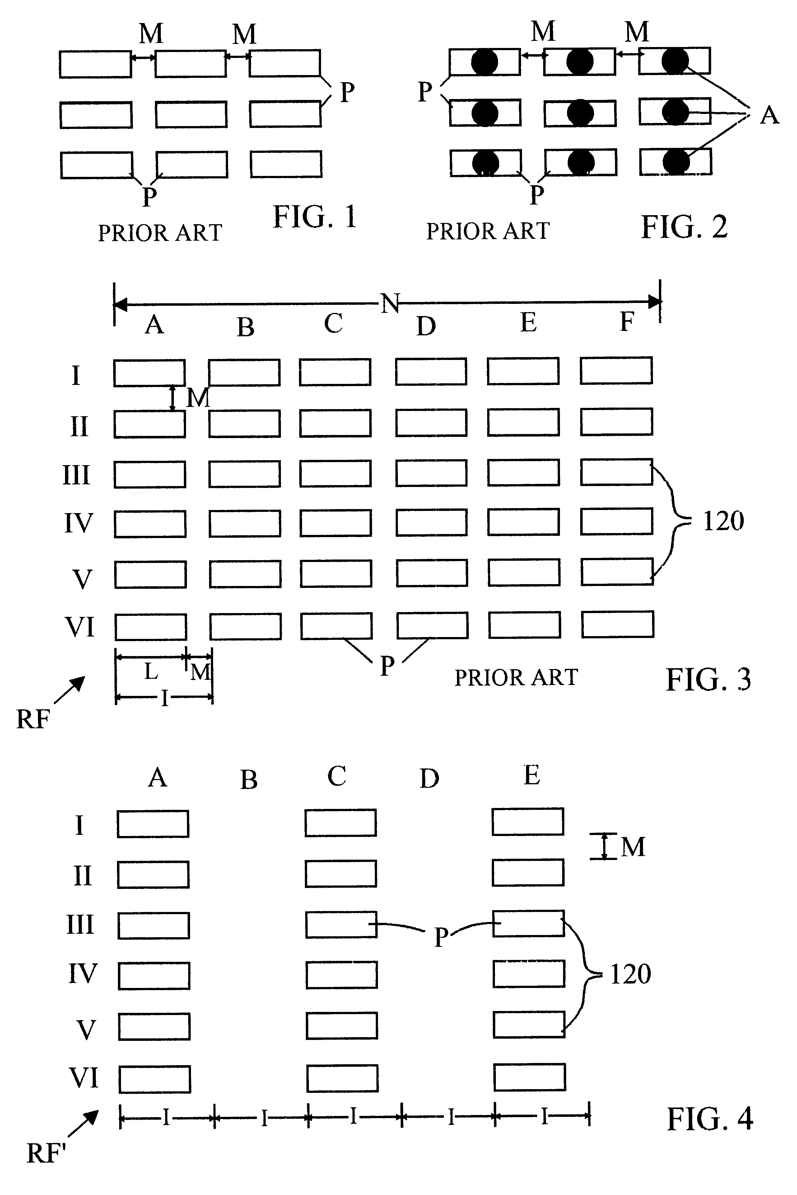
FIGS. 17 and 18A-18C illustrate a modification of the invention employing a plurality (three) nanosteps with a reticle mask RF". The reticle mask RF" is adapted to triple exposures for each field exposed on the workpiece. This embodiment of the invention shows how the invention may be employed when the original reticle mask is deconstructed to require "n" exposures for each field where "n" is a positive integer. In this case n=3.
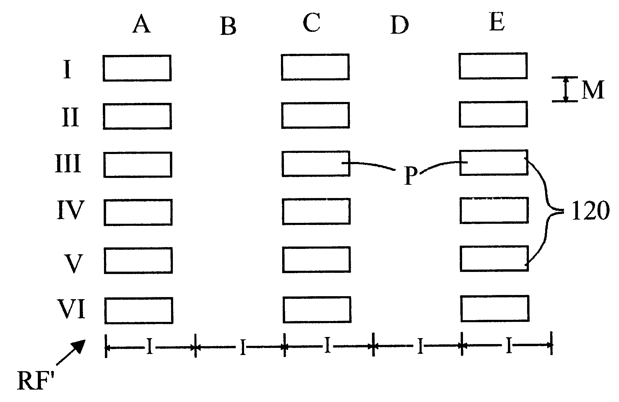
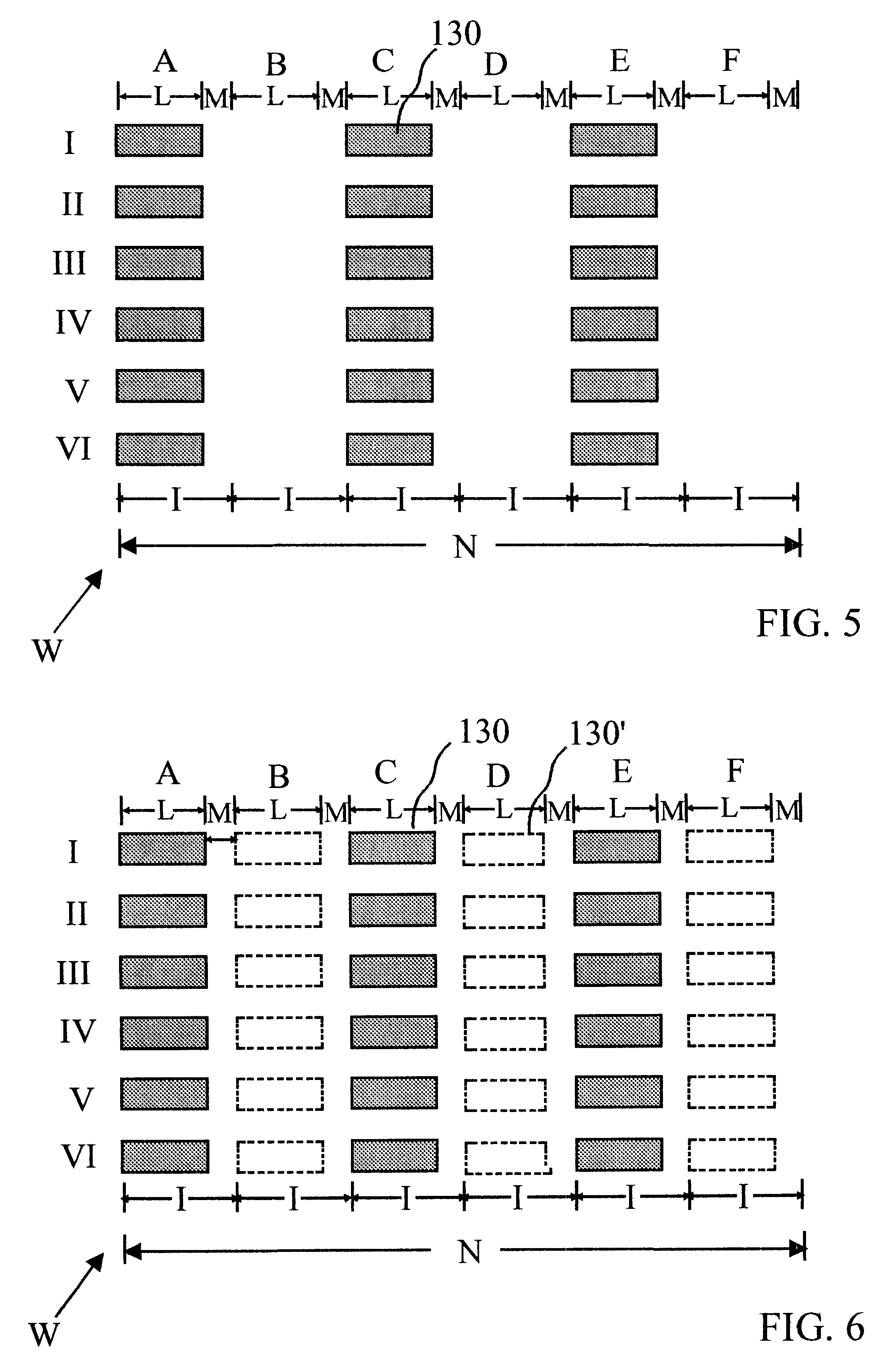
FIG. 17 shows a reticle mask RF" which has a mask layout that is a modification of the layout shown in FIG. 4. The layout of reticle mask RF" of FIG. 17 is suitable for use an interleaved triple exposure process using a single reticle mask and intermediate two nanosteps between exposures to form the pattern shown in FIG. 3 in accordance with the method of this invention.
FIGS. 18A, 18B and 18C illustrate a triple exposure process used to form final desired pattern in accordance with this invention by "nanostepping" in which distances of stage movement are qui...
PUM
| Property | Measurement | Unit |
|---|---|---|
| length | aaaaa | aaaaa |
| distance | aaaaa | aaaaa |
| distances | aaaaa | aaaaa |
Abstract
Description
Claims
Application Information