Method and apparatus for thermal control of a semiconductor substrate

Inactive Publication Date: 2002-10-15
APPLIED MATERIALS INC
View PDF2 Cites 57 Cited by
  • Summary
  • Abstract
  • Description
  • Claims
  • Application Information

AI Technical Summary

Benefits of technology

To facilitate understanding, identical reference numerals have been used, wh

Problems solved by technology

Changes in, and gradients across the wafer surface during wafer processing are detrimental to material deposition, etch rate, feature taper angles, step coverage and the like.
This method of cooling the wafer has two inherent problems.
First, the response time required to bring a wafer to a desired temperature is relatively long.
As such, rapid dynamic control of the water temperature to compensate for rapid wafer te

Method used


Image

  • Method and apparatus for thermal control of a semiconductor substrate
  • Method and apparatus for thermal control of a semiconductor substrate
  • Method and apparatus for thermal control of a semiconductor substrate

Examples


Example

A second embodiment of 
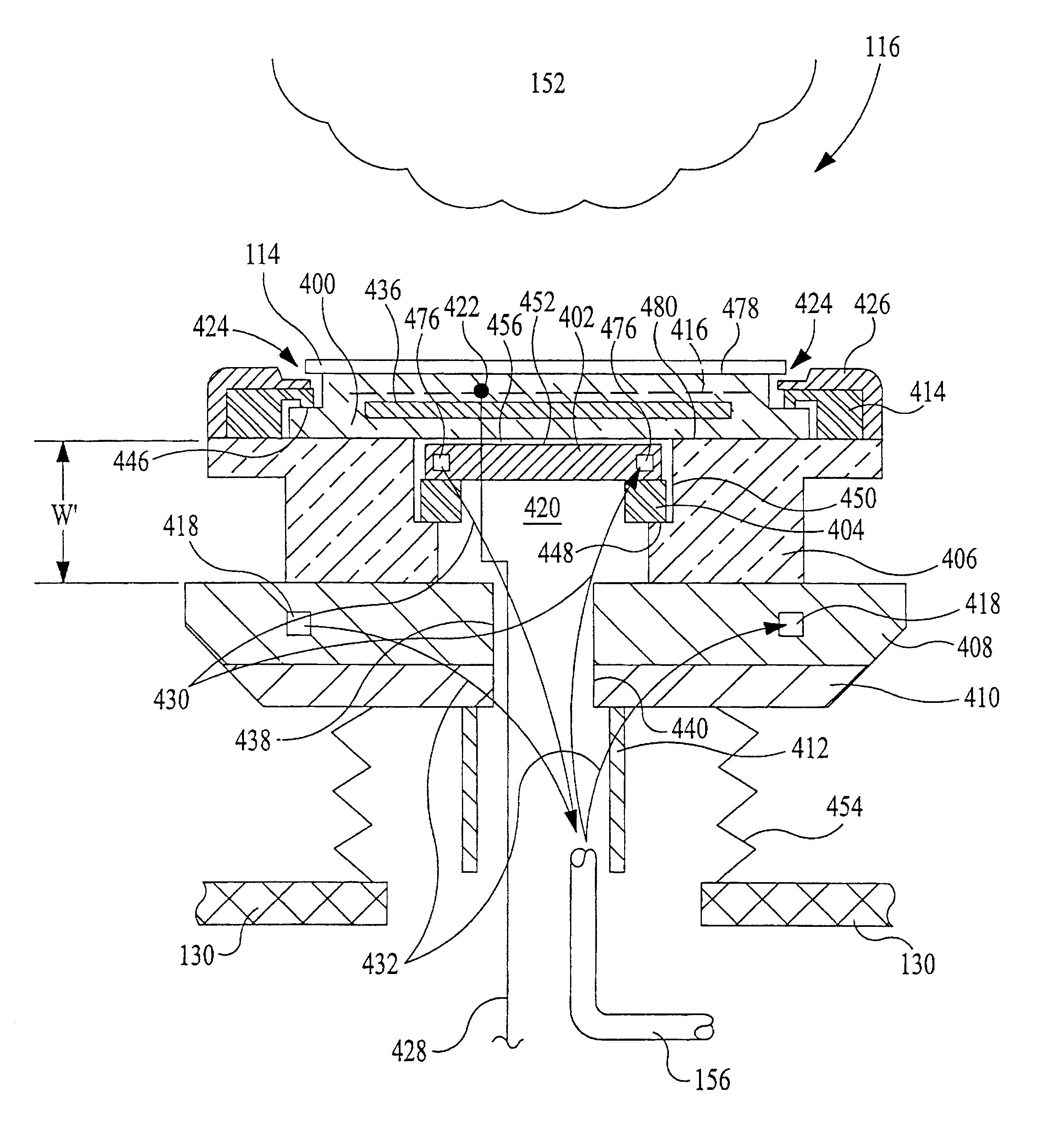
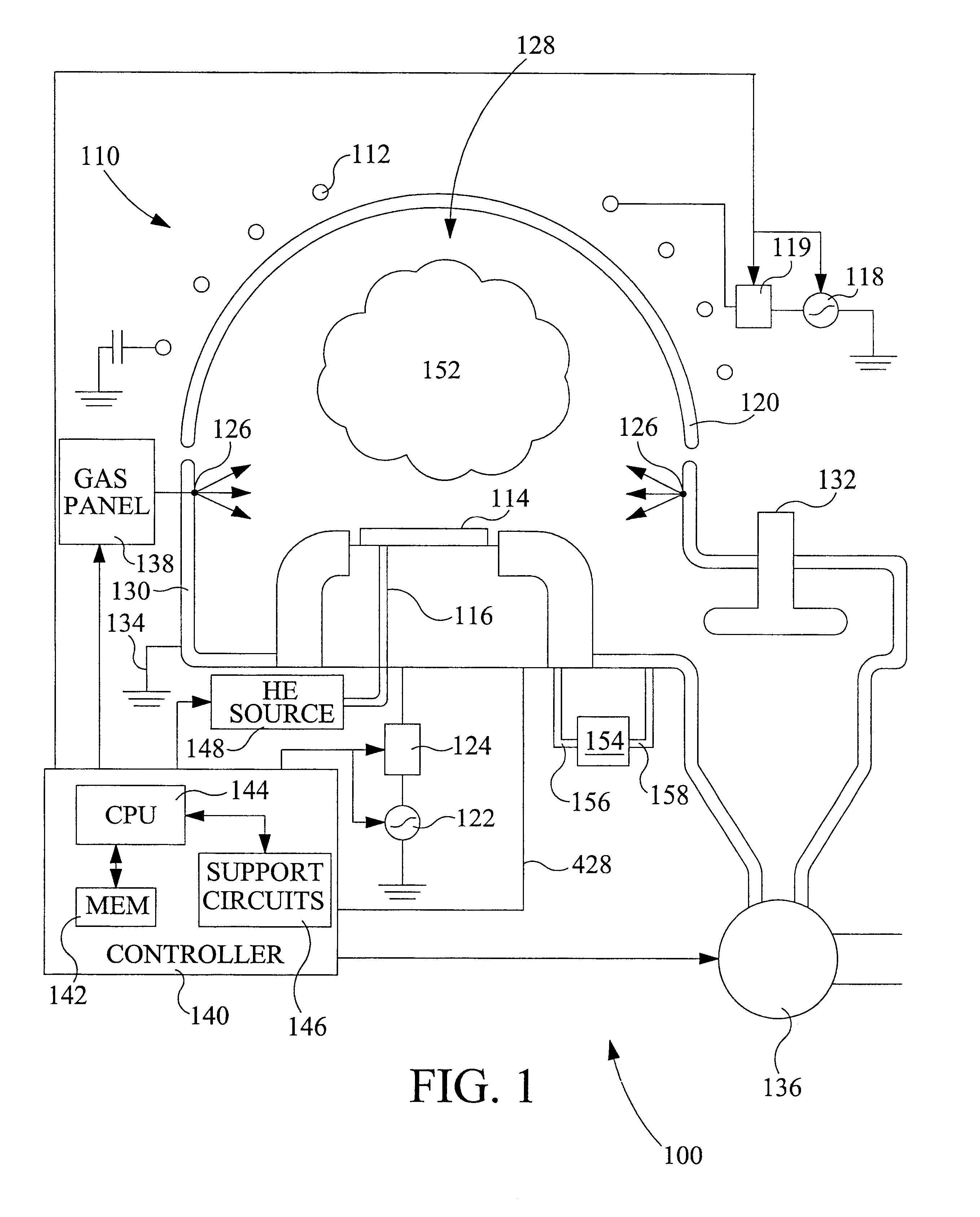
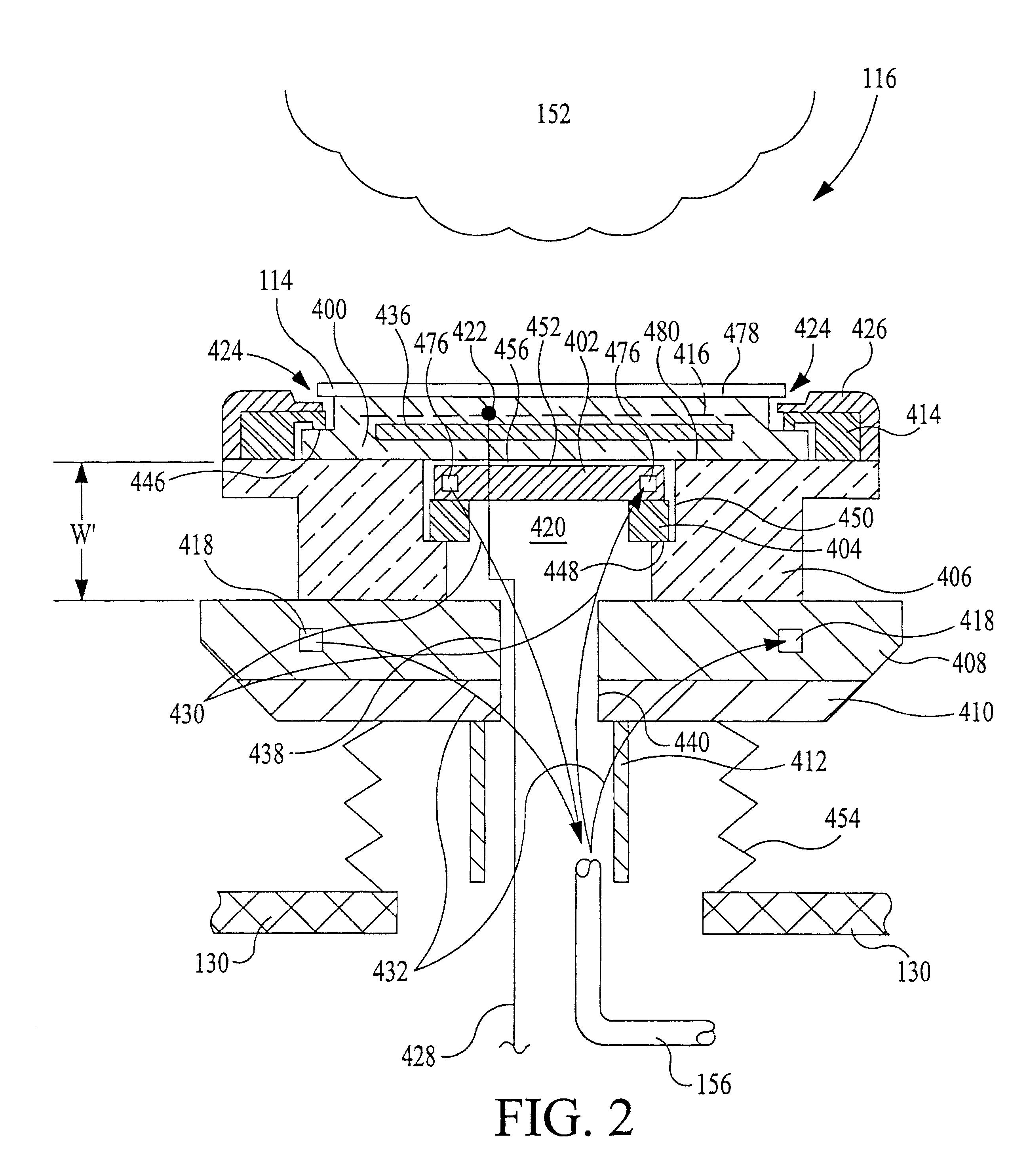
the support pedestal 116 is depicted in FIG. 3. The support pedestal 116 comprises a substrate support 400, an internal heat transfer plate 300, an isolator 466, an external heat transfer plate 408, a housing 410, a shaft 412 and clamp 414. The substrate support 400 can be an electrostatic chuck, a heater, a ceramic body or the like. A sensor 422 is positioned in the substrate support 400 near a substrate side 478. The sensor 422 is coupled to the controller 140. The clamp 414 holds the flange 446 of substrate support 400 against the isolator 466. The clamp 414 is fastened to the isolator 466 typically by bolts (not shown). A cover ring 426 is disposed above the clamp 414. The cover ring 426 protects the clamp 414 and exposed portion 424 of the substrate support 400 from being etched by the plasma 152.

One or more electrodes are embedded in the substrate support 400. The one or more electrodes may be used for various requirements of semiconductor substrate proc...


PUM


Abstract

A semiconductor wafer processing apparatus, and more specifically, a semiconductor substrate support pedestal having a substrate support, an isolator, and first and second heat transfer plates for providing a controllable, uniform temperature distribution across the diameter of a semiconductor wafer. A semiconductor wafer placed upon the pedestal is maintained uniformly at a predetermined temperature by heating the wafer with one or more electrodes embedded within the substrate support and cooling the wafer with a fluid passing through the first and second heat transfer plates.

Description

BACKGROUND OF THE DISCLOSURE1. Field of InventionThe present invention relates generally to a semiconductor wafer processing apparatus. More specifically, the invention relates to a semiconductor support pedestal for providing a controllable, uniform temperature distribution across the diameter of a semiconductor wafer.2. Background of Prior ArtIn semiconductor wafer processing, the surface temperature of the wafer is a critical process parameter. Changes in, and gradients across the wafer surface during wafer processing are detrimental to material deposition, etch rate, feature taper angles, step coverage and the like. It is essential to have control over temperature uniformity during wafer processing to enhance processing and minimize undesirable characteristics.A number of devices have been used in the art to control wafer temperature during processing. One method feeds a chilled fluid through a wafer support pedestal during wafer processing. The fluid removes heat from the wafer...

Claims


Application Information

Patent Timeline
IPC IPC(8): H01L21/00H01L21/67H01L21/687H01L21/302H01L21/205H01L21/3065H01L21/68
CPCH01L21/67098H01L21/68785Y10T279/23H01L21/68
Inventor MOK, YEUK-FAI EDWINLUBOMIRSKY, DMITRYKOOSAU, DENNISWANG, DANNYTHACH, SENHEXLINE, PAUL
Owner APPLIED MATERIALS INC
Why Eureka
Try Eureka