Addressable fuse array for circuits and mechanical devices

a fuse array and circuit technology, applied in the field of fuse arrays, can solve the problems of impracticality of using such prior art microbridge fuses for customizing mechanical properties, imposing a large burden on designers and fabricators, and high cost of secondary fabrication steps

Inactive Publication Date: 2002-12-31
MICROSOFT TECH LICENSING LLC
View PDF7 Cites 106 Cited by
  • Summary
  • Abstract
  • Description
  • Claims
  • Application Information

AI Technical Summary

Problems solved by technology

These requirements imposes a large burden on designers and fabricators, particularly for large-scale integrated circuits.
While feasible, such secondary fabrication steps are expensive.
Further, these prior art fuses are only used for electrical connections.
Because each fuse must be separately addressed, which requires a large number of electrodes, the use of such prior art microbridge fuses for customizing mechanical properties is impractical.
Customizing the resonate filter after incorporation into a circuit has heretofore been substantially impractical.
This requirement increases cost and makes prohibitively expensive the use of such mechanical filters in anything other than large scale fabrication.
Thus, although resonators are know in the prior art, an obstacle to their use on circuits, and in MEMS, is the problem of tuning the resonator for a desired parameter, such as a center frequency or bandwidth where the resonator is to be used as a filter.

Method used


Image

  • Addressable fuse array for circuits and mechanical devices
  • Addressable fuse array for circuits and mechanical devices
  • Addressable fuse array for circuits and mechanical devices

Examples


third embodiment

A third embodiment is shown in FIG. 8. This embodiment includes the comb drives 106a and 106b and the masses 102a and 102b as described above in connection with other embodiments. In this embodiment, however, the coupler 122, located between the masses 102 does not include fuse portions. Rather, the coupler 122 is shown fixedly coupled to the masses in an exemplary configuration.

Bias members 116a-116d are coupled between conductive regions 105g and 105h and a frame 142. The frame 142 is also fixedly coupled to the second combs 112 of respective comb drives 106a and 106b and the respective masses 102a and 102b. Electrical pads 102f and 120g are also located on the conductive regions 105g and 105h, respectively and are in electrical communication with the bias members via respective conductive regions 105. As in the above embodiments, the bias members 116 are conductive.

Electrical input pads 120e and 120h are coupled to the first combs 108 for driving the respective comb drives 106a a...


PUM


Abstract

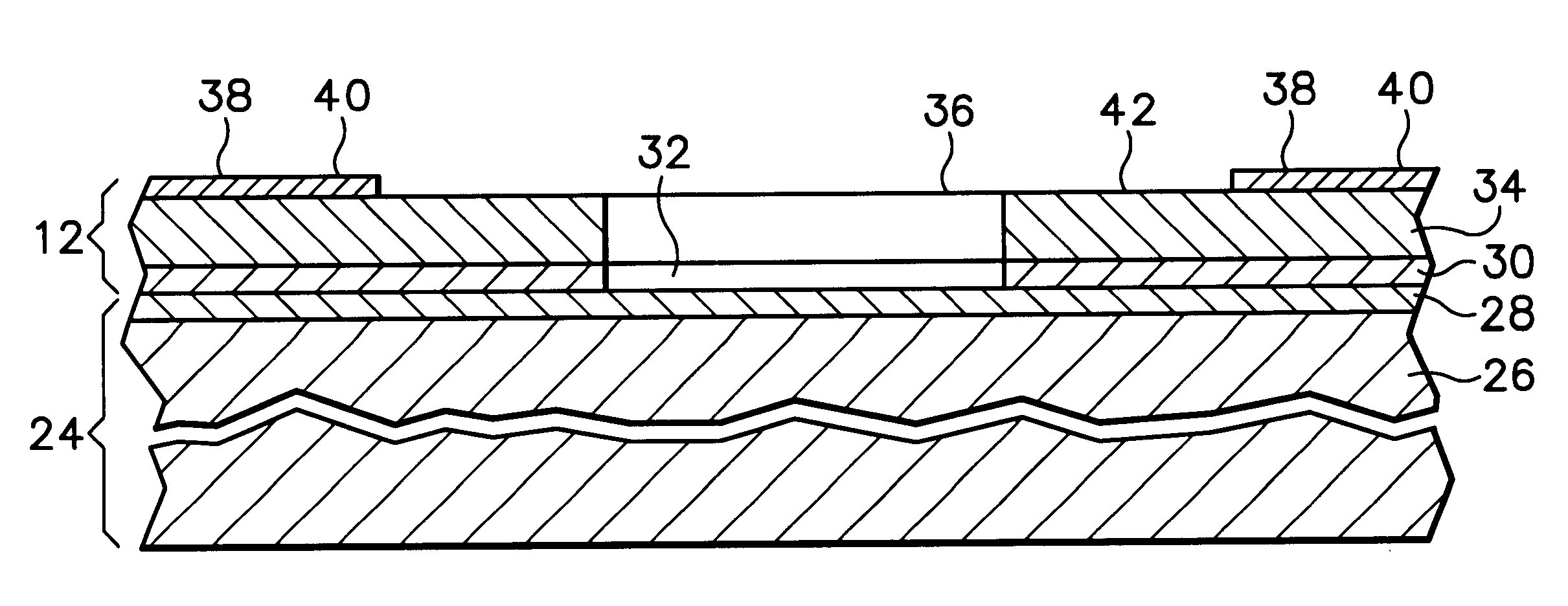
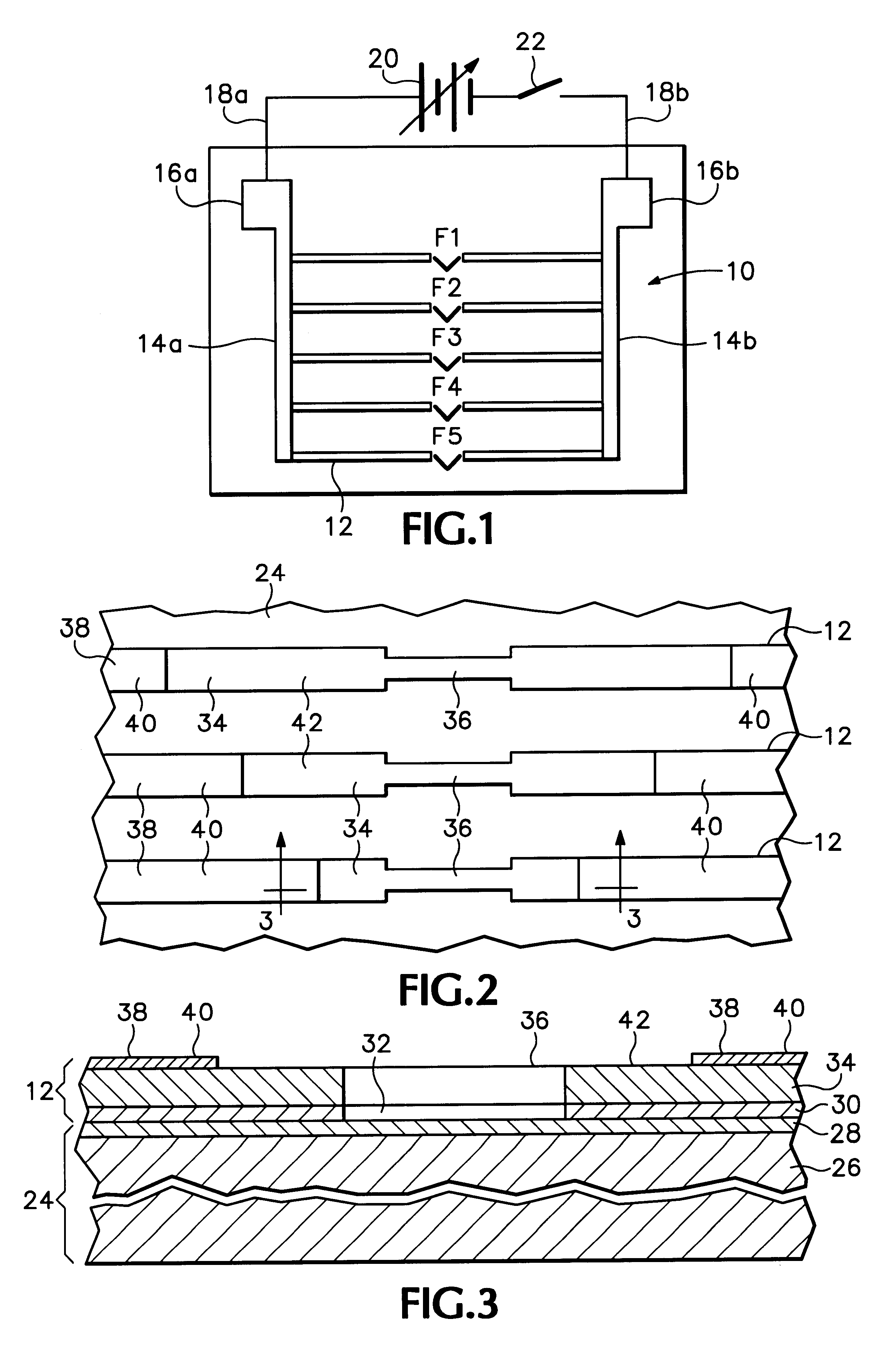
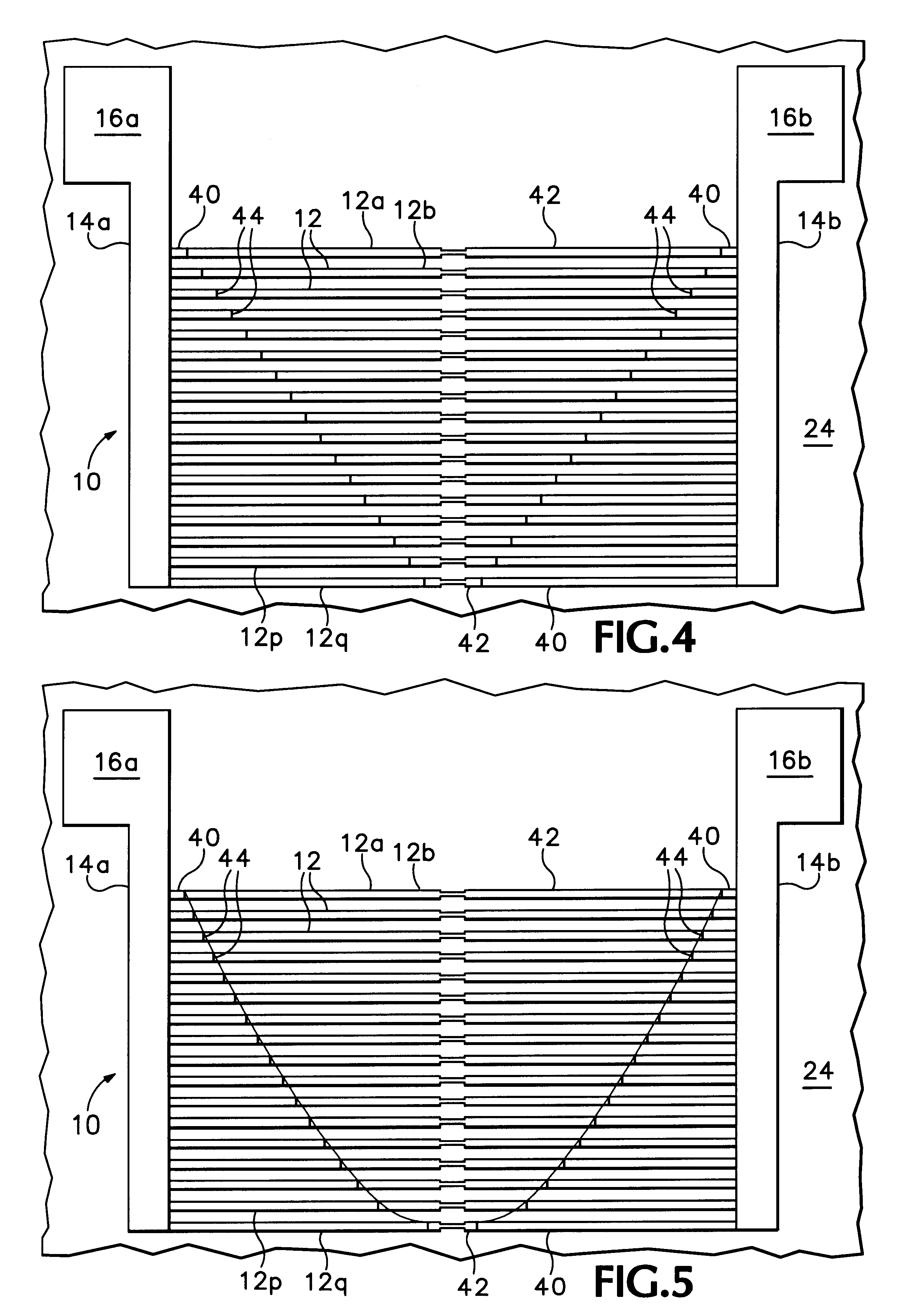
A fuse array having a plurality of fusible links that can be addressed by two electrodes is disclosed. The fuse array includes two conductive strips having the plurality of fusible links located therebetween and electrically coupled to the conductive strips. The fusible links have different electrical resistance and each fusible link includes a fuse portion. A voltage potential applied across the conductive strips induces current flow through the fusible links in accordance with Ohm's law and ohmic heating occurs at the fuse portion in proportion to the square of the current. The voltage is increased to cause sufficient ohmic heating to occur in the most conductive fusible link (the fusible link having the lowest electrical resistance) so that the fuse portion in that fusible link fuses. Because the fusible links are connected in parallel to the conductive strips, an equivalent resistance of the plurality of fusible links increases and the current flow diminishes so that no further fuse portions are fused at the selected voltage level. Thereafter, the voltage level may be increased to fuse the most conductive fusible link remaining that is not fused. The fuse array may be incorporated into a circuit as a resistor that can be tuned to circuit requirements or as a physical structure in MEMS devices wherein the fuse array may be tuned to change physical properties of the MEMS device.

Description

1. Field of the InventionThis invention pertains to fuse arrays, and more particularly fuse arrays that can be fabricated on integrated circuits and electrically modified to vary their electrical and mechanical properties.2. Description of the Related ArtA fusible link is an electrical conductor that can be melted, or broken, by ohmic heating. Fusible links, or simply, fuses, are common in consumer electronics to prevent circuit damage that can be caused by excess current. Thus, in a fused circuit, the fuse provides an electrical path within the circuit that acts as a normal conductor until a predetermined amount of excess current attempts to pass through the fuse. The excess current causes the fuse to heat excessively until the fuse fuses, i.e., melts or breaks, thereby creating an open circuit to prevent damage to other circuit components.A polysilicon micro-fuse 2 is known in the art and shown in FIG. 12. Known as a resistive microbridge fuse, this fuse includes enlarged ends 4 c...

Claims


Application Information

Patent Timeline
Patent Type & Authority Patents(United States)
IPC IPC(8): B81B7/00H01L23/525H01L23/52B81B3/00
CPCB81B3/0086B81B7/0012H01L23/5256H01L2924/0002H01L2924/00
Inventor SINCLAIR, MICHAEL J.LEVITAN, JEREMY A.
Owner MICROSOFT TECH LICENSING LLC
Why Eureka
Try Eureka