
Liquid crystal display element integrated with a touch sensor

a technology of touch sensor and display element, which is applied in the direction of identification means, instruments, computing, etc., can solve the problems of difficult to compact and light weight an electronic apparatus, the weight of the whole element is shortened, and the effect of reducing the size of the electronic apparatus

Inactive Publication Date: 2002-12-31
AU OPTRONICS CORP
View PDF4 Cites 389 Cited by
  • Summary
  • Abstract
  • Description
  • Claims
  • Application Information

AI Technical Summary

Problems solved by technology

This has resulted in thickening and weighting of the whole of the element.
Additionally, this has resulted in creating an optically undesirable condition owing to degradation of performance such as transmissivity.
For this reason, it has been difficult for an electronic apparatus required to be compact and light weight such as a note book type personal computer to be equipped with a touch sensor unit.
Moreover, since a touch sensor unit of this kind is fabricated in a different process from that for a liquid crystal element, its cost has also increased.
This has improved the problem of thickness and weight to some extent, but it is unsatisfactory.
Moreover, using a film has caused increase of cost conversely because of complexity of a fabricating process of a conductive thin film, as compared with a fabricating process of a glass substrate.
And lack of strength and optical non-uniformity of a film has made it impossible to fabricate a touch sensor unit exhibiting full reliability and optical characteristics.

Method used


Image

  • Liquid crystal display element integrated with a touch sensor
  • Liquid crystal display element integrated with a touch sensor
  • Liquid crystal display element integrated with a touch sensor

Examples


Embodiment Construction

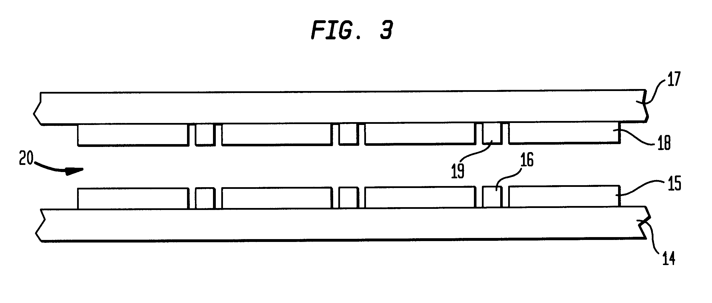
FIG. 3 is a cross-sectional view showing an example of a liquid crystal display element integrated with a touch sensor of the present invention. A first display electrode 15 and a first touch electrode 16 are provided on a first substrate 14, and a second display electrode 18 and a second touch 19 electrode are provide on a second substrate 17. A liquid crystal layer 20 is interposed between the first substrate 14 and the second substrate 17. The present invention can be applied to a liquid crystal display apparatus of both a reflective type and a transparent type.

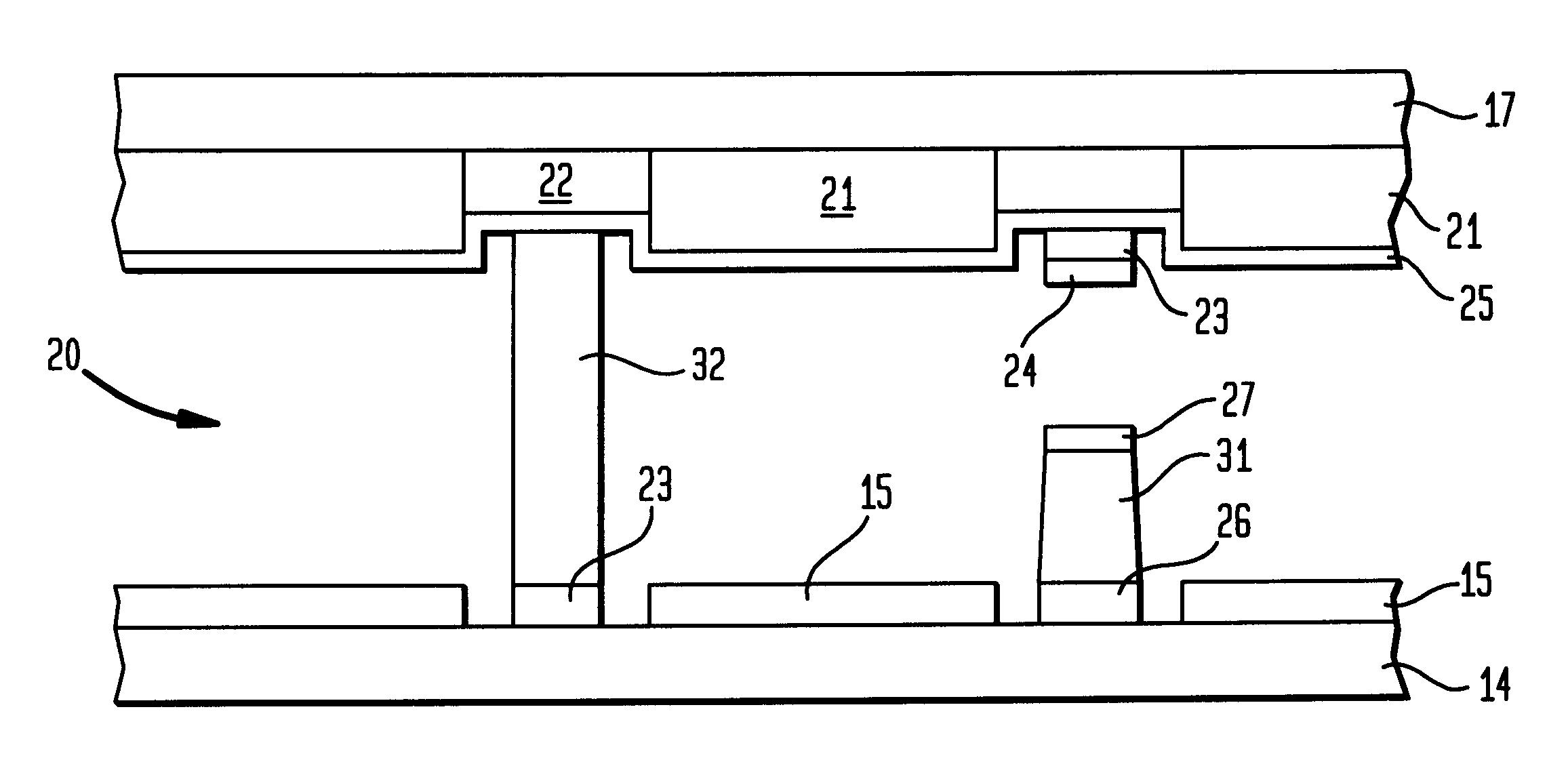
FIG. 4 is a cross-sectional view showing another example of a liquid crystal display element integrated with a touch sensor of the present invention. The first display electrode 15 is formed on the first substrate 14. In FIG. 4, the first display electrode 15 is indicated as a pixel electrode. A color filter layer 21 and a black matrix layer 22 are provided on the second substrate 17, and the second display electrode 25 is...


PUM

PropertyMeasurementUnit
heightaaaaaaaaaa
heightaaaaaaaaaa
heightaaaaaaaaaa

Abstract

The present invention provides a newly constituted liquid crystal display element incorporating a touch sensor unit.In a liquid crystal display element where a liquid crystal layer is inserted between a first substrate and a second substrate, a display electrode for displaying an image and a touch electrode for detecting a touch position are provided on the surfaces of the first substrate and the second substrate opposing with each other. The display electrode may be used as the touch electrode. A pillar-shaped spacer may be formed to support the first substrate and the second substrate. Additionally, the touch electrode may be provided on a convex-shaped part formed on the substrate.

Description

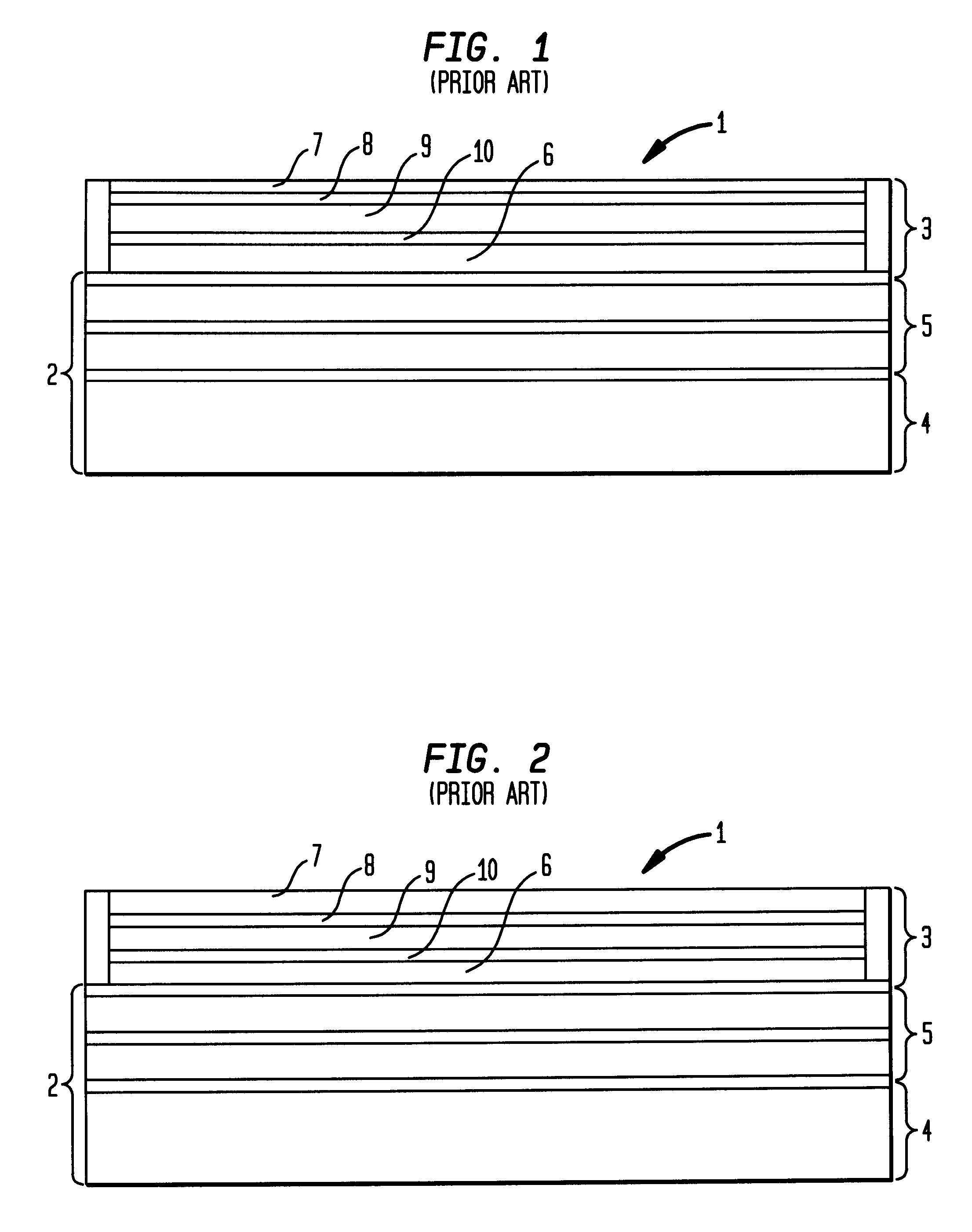
1. Technical FieldThe present invention relates to a liquid crystal display element integrated with a touch sensor, more particularly to a liquid crystal display element integrated with a touch sensor using a resistive membrane method.2. Prior ArtHeretofore, it has been necessary to add a touch sensor unit as an external component to a liquid crystal display element when a touch panel function is given to the liquid crystal display element using, for example, a resistive membrane method.FIG. 1 shows a liquid crystal display apparatus 1 having a conventional touch sensor function. That is, an upper electrode 8 is formed on a film 7 and a lower electrode 10 is formed on a glass substrate 6. By laminating the film 7 and the glass substrate 6 via a spacer, a touch sensor unit 3 of the resistive membrane method is formed. There is a space 9 between the upper electrode 8 and the lower electrode 10. Then, this touch sensor unit 3 is attached externally to a liquid crystal display element 2...

Claims


Application Information

Patent Timeline
Patent Type & Authority Patents(United States)
IPC IPC(8): G02F1/133G02F1/13G06F3/033G02F1/1339G06F3/041G02F1/1333G06F3/045G09F9/00H01H13/712
CPCG02F1/13338G06F3/0412G06F3/045G02F1/13394
Inventor KURIHARA, MIKIOKANZAKI, EISUKEKIYOOKA, FUMITOSHI
Owner AU OPTRONICS CORP
Learn More