Display device

a technology of display device and display angle, which is applied in the direction of static indicating device, identification means, instruments, etc., can solve the problem of limited viewing angle range of liquid crystal display devi

Inactive Publication Date: 2003-02-11
INTELLECTUAL KEYSTONE TECH LLC
View PDF23 Cites 113 Cited by
  • Summary
  • Abstract
  • Description
  • Claims
  • Application Information

AI Technical Summary

Problems solved by technology

In general, a liquid crystal display device has a problem of a limited viewing angle range due to a marked change in the transmissivity or the reversal of gray scale in a direction of a viewing angle that deviates from the direction of the normal line with respect to a display surface.
In such a case

Method used


Image

  • Display device
  • Display device
  • Display device

Examples


first embodiment

(First Embodiment)

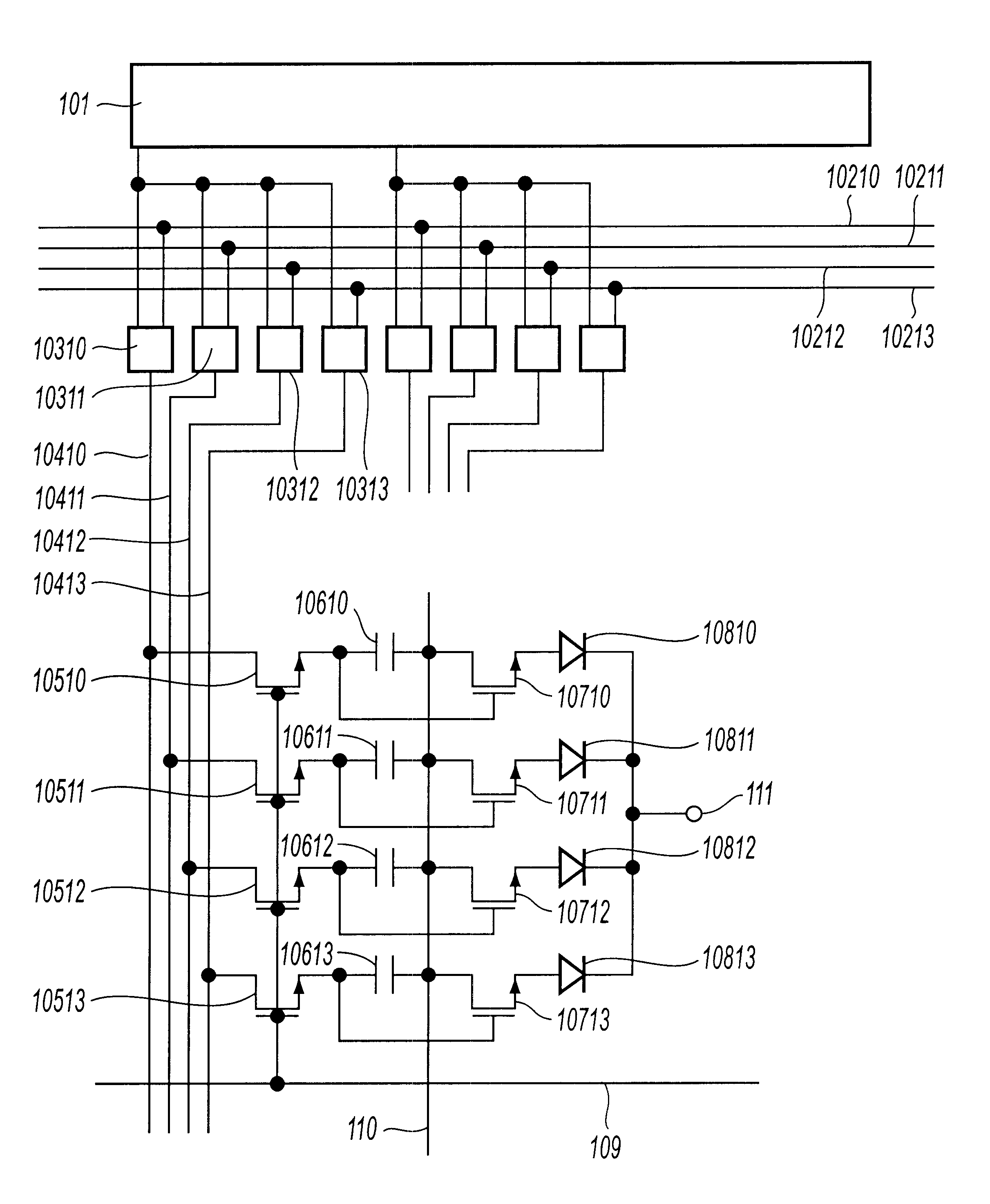
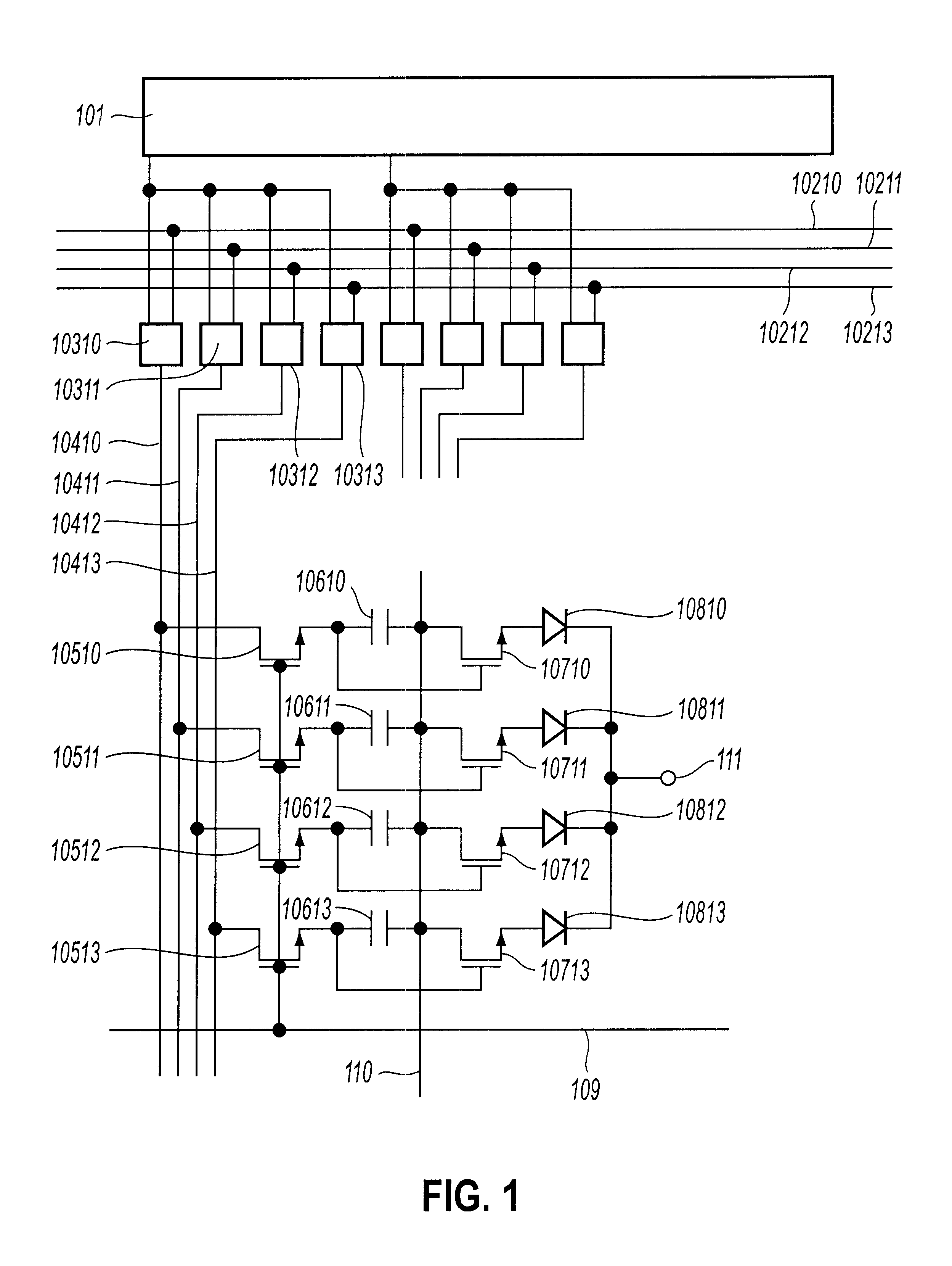
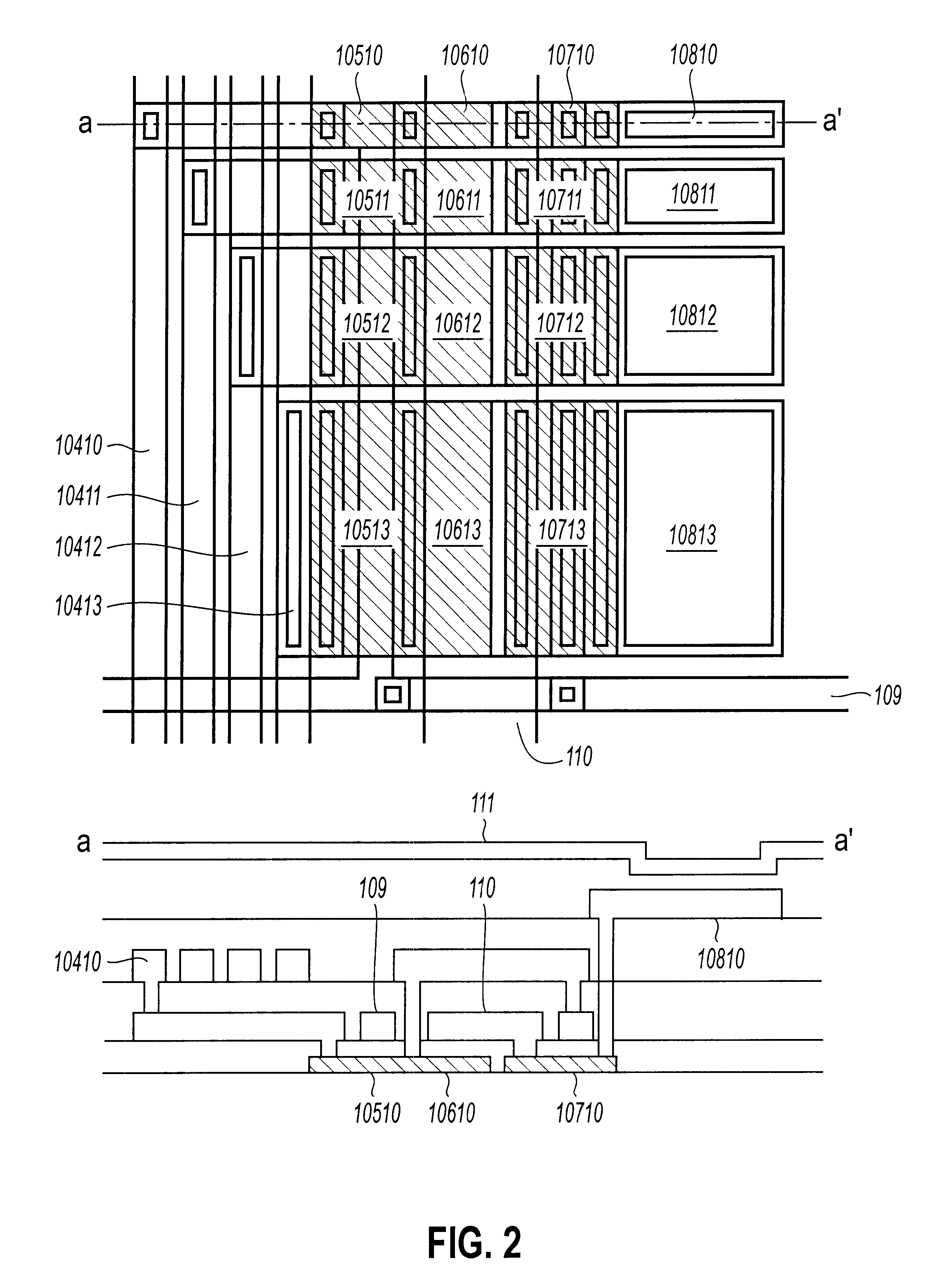
FIG. 1 is an equivalent circuit diagram of a TFT-OELD of a first embodiment in accordance with the present invention. Although only one pixel is shown in the drawing, there are many pixels arranged in a plurality of rows and a plurality of columns in an actual device.

When a pulse is output from a shift register 101, digital signals of digital signal supply lines 10210 through 10213 of zero-th through third bits are transmitted to source lines 10410 through 10413 via transmission switches 10310 through 10313 of the zero-th through third bits. In other words, the digital signals are transmitted to each pixel. For a gate line 109 that has been selected at this time, the digital signals are respectively transmitted to retention capacitors 10610 through 10613 of the zero-th through third bits via switching transistors 10510 through 10513 of the zero-th through third bits, respectively. Current transistors 10710 through 10713, which are thin film transistors, and organic...

second example

(Second Example)

FIG. 4 is an equivalent circuit diagram of a TFT-OELD of a second embodiment in accordance with the present invention.

The operations, functions, and advantages of the TFT-OELD of this embodiment are almost identical to those of the first embodiment. In this embodiment, however, a gate line 109 is divided into a gate line 1090 for lower-order bits that is assigned the functions of zero-th and first bits and a gate line 1091 for higher-order bits that is assigned the functions of second and third bits. This makes it possible to reduce the number of the digital supply lines and the number of the transmission switches and source lines per column from four to two. However, the frequencies of the scanning signals of the gate lines, the pulses of the shift register, and the digital signals will be doubled.

application example

(Application Example)

The present invention is intended to reduce the nonuniformity in the luminous intensity of luminescent elements caused by the nonuniformity in the conductance of transistors in a current luminescent display element and therefore it is intrinsically different from the area gray scale method of the liquid crystal display element mentioned in "Background Art." In fact, current luminescent display elements do not even need to have different areas as long as they have different luminous intensity levels. Their structures, however, have similar aspects. Therefore, many embodiments disclosed in relation to the area gray scale method of liquid crystal display elements can be applied to the gray scale method in accordance with the present invention, and the similar advantages to those of the disclosed embodiments can be expected.

Industrial Applicability

Having the advantages described above, the present invention is ideally used with a display device equipped with element...


PUM


Abstract

In a display device in accordance with the present invention, each pixel includes a plurality of luminescent elements having different luminous intensities to represent gray scales by controlling the turning ON/OFF of the luminescent elements. A digital signal is transmitted to each pixel to carry out control by thin film transistors connected in series with the luminescent elements. The luminous intensities of the luminescent elements are the geometric progressions of a common ratio of 2. The ON resistance of the thin film transistors is set to be lower than the ON resistance of the luminescent elements, while the OFF resistance of the thin film transistors is set to be higher than the OFF resistance of the luminescent elements. These features have reduced the nonuniformity in the luminous intensities of the luminescent elements caused by the nonuniformity in the conductance of the transistors, thus achieving improved image quality.

Description

1. Field of the InventionThe present invention relates to a display device equipped with a display element and, more particularly, to a display device equipped with an element that emits light by means of a thin film transistor and current (hereinafter referred to as a "current luminescent display device".2. Description of the Related ArtA thin film transistor organic electroluminescent device (hereinafter referred to as "TFT-OELD") may be cited as a highly promising future current luminescent display device that realizes a larger size, higher definition, a wider viewing angle, and reduced power consumption.A method for driving a typical conventional TFT-OELD will be described.FIG. 5 shows an equivalent circuit of the conventional TFT-OELD. Only one pixel is shown in the drawing although there are actually many pixels in a plurality of rows and a plurality of columns.A pulse is output from a shift register 101, and an analog signal of an analog signal supply line 1022 is transmitted...

Claims


Application Information

Patent Timeline
IPC IPC(8): G09G3/32G09G3/30G09F9/30G09G3/20H01L51/50
CPCG09G3/2074G09G3/3258G09G3/3291G09G2320/0233G09G2300/0852G09G2310/027G09G2300/0417G09G3/30
Inventor KIMURA, MUTSUMI
Owner INTELLECTUAL KEYSTONE TECH LLC
Why Eureka
Try Eureka