Method of designing layout for integrated circuit

a layout and integrated circuit technology, applied in the direction of cad circuit design, program control, instruments, etc., can solve the problems of short circuit of signal lines, deterioration of relative skew of clock signals, and unconnected terminals,

Inactive Publication Date: 2003-02-11
NEC ELECTRONICS CORP
View PDF5 Cites 18 Cited by
  • Summary
  • Abstract
  • Description
  • Claims
  • Application Information

AI Technical Summary

Problems solved by technology

As explained above, with the prior-art layout method as shown in FIG. 2, there is a problem that short-circuit of the signal lines tends to occur and as a result, the re-routing operation of the clock lines is essentially required to eliminate the short-circuited signal lines.
Moreover, because of the re-routing operation of the clock lines, the relative skew of the clock signal that has been adjusted to be minimized or optimized through the CTS process is changed, resulting in another problem that the relative skew of the clock signal deteriorates.
Unless the re-routing operation is not conducted, there is a further problem that short-circuited signal lines and unconnected terminals may be left.
the prohibited areas causing an obstacle to define layout of signal lines in each of the wiring layers if a clock line is defined to intersect at least one of the prohibited areas;
Moreover, since there is no possibility to redefine the optimized layout of the clock lines, the relative skew of the clock signal is optimized or minimized.
the prohibited areas causing an obstacle to define layout of signal lines if clock lines are defined to intersect the prohibited areas;
The prohibited areas cause an obstacle to define layout of signal lines if clock lines are defined to intersect the prohibited areas.
Also, since there is no possibility to redefine the optimized layout of the clock signals, the relative skew of the clock signal is optimized.
the prohibited terminals causing an obstacle to define layout of signal lines if clock lines are defined to intersect the prohibited terminals;
Thus, the re-routing operation required in the previously explained prior-art method is unnecessary, which eliminates the amendment or positional shift of the optimized layout of the clock lines through the CTS process.

Method used


Image

  • Method of designing layout for integrated circuit
  • Method of designing layout for integrated circuit
  • Method of designing layout for integrated circuit

Examples


second embodiment

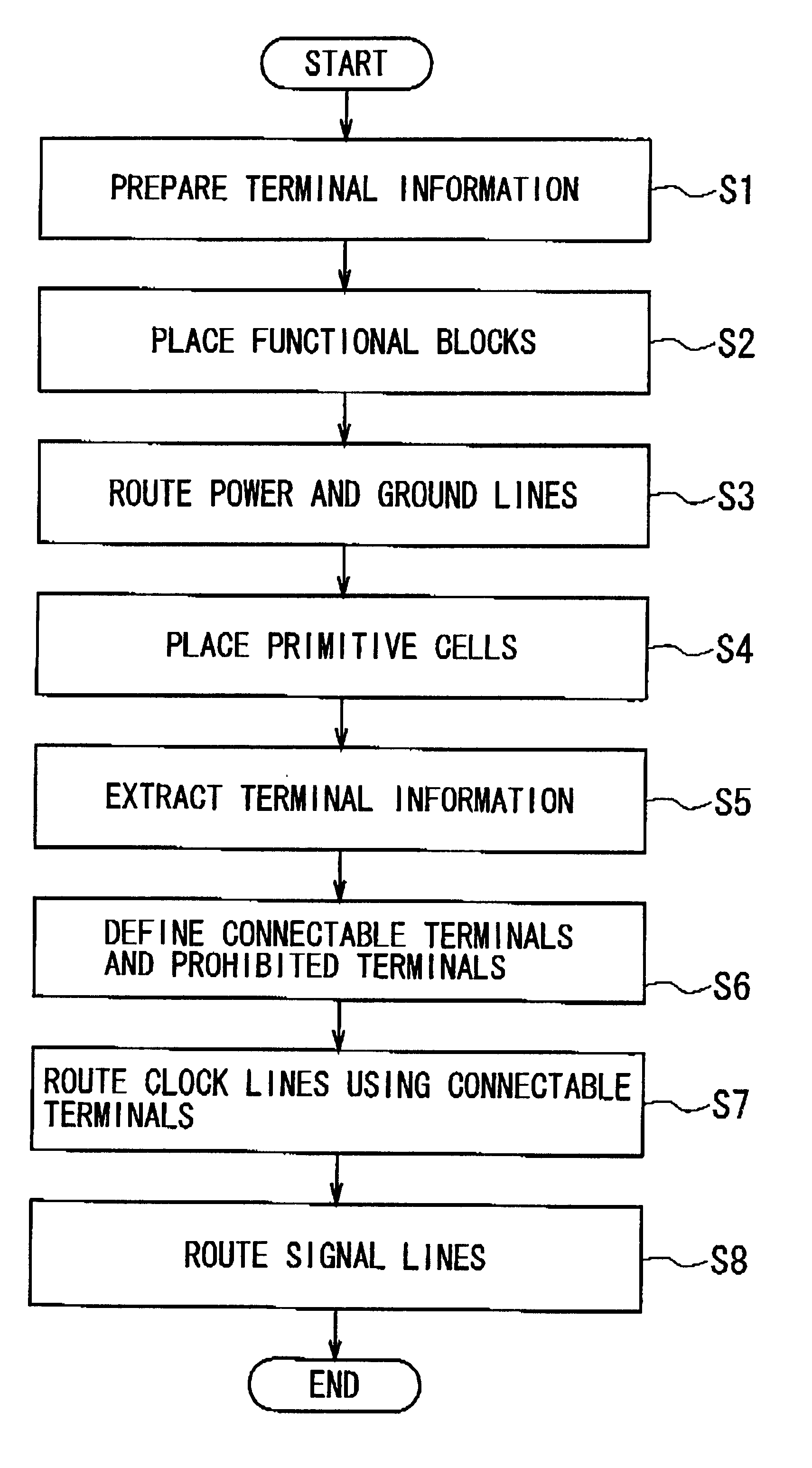
FIG. 12 shows the layout section of a CAD tool used for conducting a method of designing the layout for an IC according to the invention.

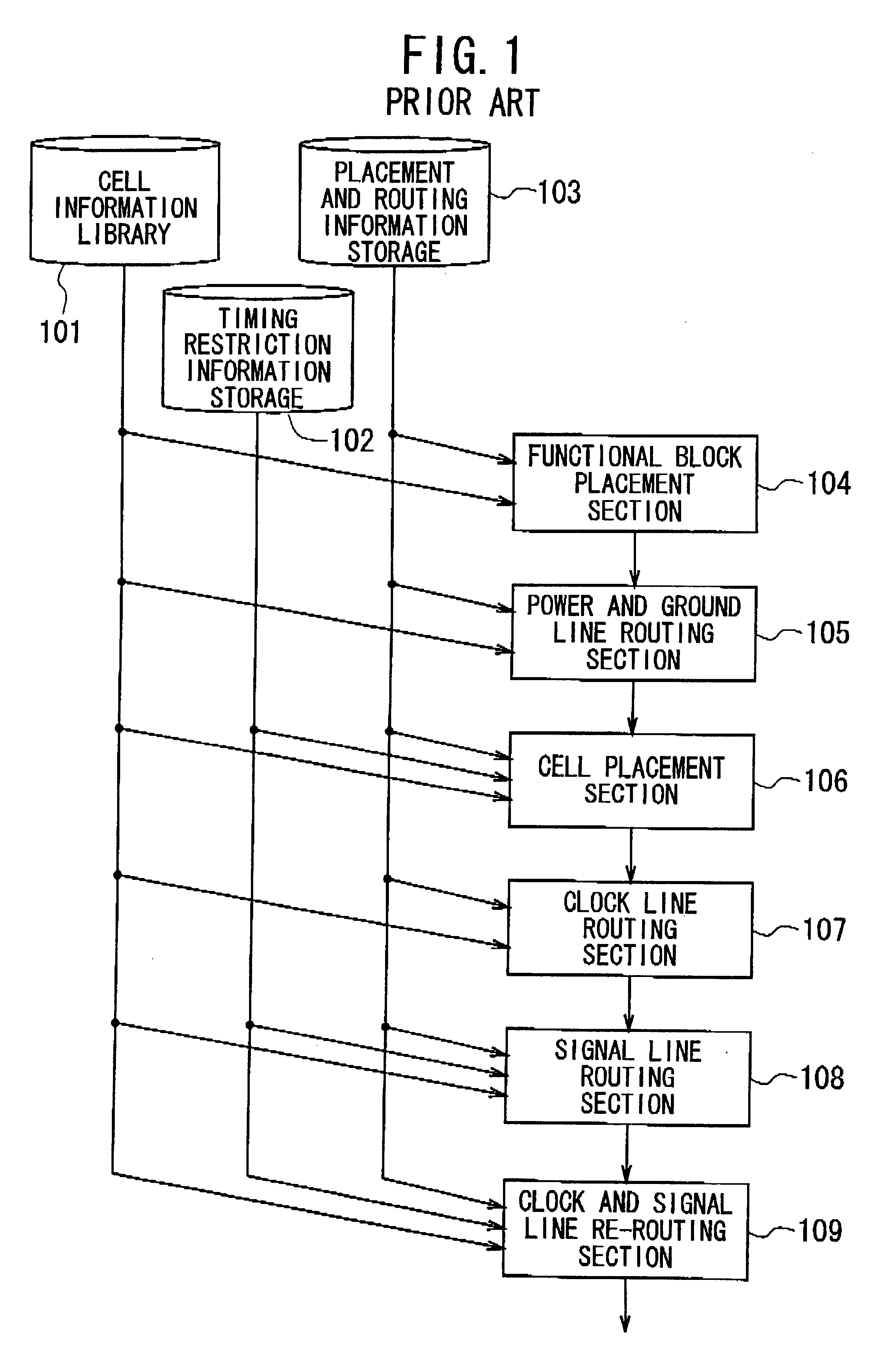
The system in FIG. 12 comprises the same configuration as the system shown in FIG. 7 used in the method according to the first embodiment, except that a prohibited terminal information library 11 is provided instead of the cell and terminal information library 10. Therefore, the detailed description about the same configuration is omitted here for the sake of simplification of description by attaching the same reference numerals as used in the first embodiment to the same elements in FIG. 12.

In the layout section of FIG. 12, the library 11 stores the information about the terminals that are prohibited from being overlapped by clock lines located in each wiring layer as the "prohibited terminal information". The "prohibited terminal information" in the library 11 is read out and sent to the clock line routing section 7 as necessary.

first embodiment

Unlike the layout section of FIG. 7 used in the first embodiment, the cell information and the wiring layer information is sent to the clock line routing section 7 from the cell information library 1.

FIG. 13 shows the process steps of the method according to the second embodiment, in which the layout system shown in FIG. 12 is used.

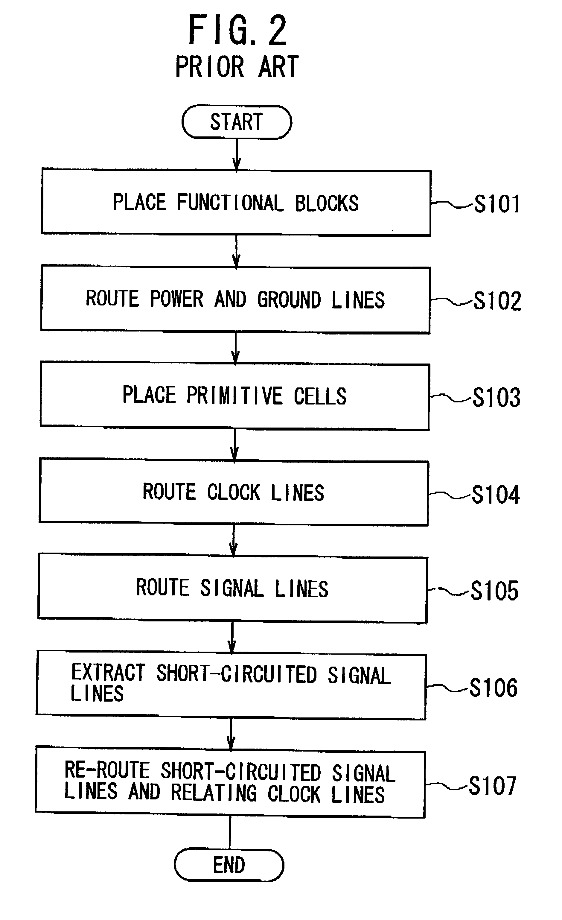
The method of the second embodiment corresponds to one obtained by replacing the steps S1, S5, and S6 in the first embodiment with the steps S11, S15, and S16, respectively. Therefore, the explanation about the same steps as shown in the first embodiment is omitted here.

In the method according to the second embodiment, first, the "prohibited terminal information" is prepared and stored in the library 11 in the step S11. For example, as shown in FIG. 14, a primitive cell 23 has prohibited terminals 13b, 14b, and 15b. In this case, the "prohibited terminal information" contains the definition or identification code that defines the terminals 13b, 14b, and 1...


PUM


Abstract

A method of designing the layout for an IC is provided, which eliminates the signal line re-routing process and which optimizes the relative skew of the clock signal. This method comprises the steps of: (a) determining prohibited areas in each of stacked wiring layers; the prohibited areas causing an obstacle to determine layout of signal lines in each of the wiring layers if clock lines are defined to intersect the prohibited areas; (b) defining layout of clock lines in each of wiring layers through a Clock Tree Synthesis process in such a way that none of the clock lines intersects the prohibited areas; and (c) defining layout of signal lines in each of the wiring layers after the step (b). Preferably, prohibited area information about a primitive cell including at least one of the prohibited areas is provided, where the prohibited area information is used in the CTS process in the step (b).

Description

1. Field of the InventionThe present invention relates to a method of designing integrated circuits (ICs) and more particularly, to a method of designing the layout for ICs using a Computer-Aided Designing (CAD) system or tool, which makes it possible to route the signal lines without their re-routing process.2. Description of the Related ArtConventionally, well-known Application Specific Integrated Circuits (ASICs) termed Gate Arrays, Standard Cells, and so on have been designed using a CAD tool, in which the Clock Tree Synthesis (CTS) process has become to play an important role. The CTS process is a process to control the propagation delay of a clock signal by assigning a clock driver (i.e., buffer) to each cell array to thereby adjust the delay with the extra capacitance and resistance added by the driver.With the CTS process, the clock lines for the respective blocks or cells are synthesized in the form of a tree and then, buffers having high driving capability are assigned to ...

Claims


Application Information

Patent Timeline
Patent Type & Authority Patents(United States)
IPC IPC(8): G06F17/50H01L21/82
CPCG06F17/5068G06F30/39
Inventor YAMASHITA, KATSUHIRO
Owner NEC ELECTRONICS CORP
Why Eureka
Try Eureka