Method of precision fabrication by light exposure and structure of tunable waveguide bragg grating

a technology of tunable waveguide bragg grating and light exposure, which is applied in the direction of glass making apparatus, manufacturing tools, instruments, etc., can solve the problems of fiber bragg gratings restricting optical network design and implementation, slow reconfiguration, and notoriously difficult to achieve optical networks

Inactive Publication Date: 2003-02-18
INTEL CORP
View PDF5 Cites 89 Cited by
  • Summary
  • Abstract
  • Description
  • Claims
  • Application Information

AI Technical Summary

Problems solved by technology

Despite their use, fiber Bragg gratings do restrict optical network design and implementation.
Optical networks are notoriously difficult to achieve and slow to reconfigure.
These solutions are difficult to implement and limit optical device design and dimensions.
Unfortunately, using PLC technology to form a large-scale integrated optical chip has proved difficult, and one of the main problems arises with forming Bragg gratings on a PLC.
The former process is susceptible to grating periodicity errors in Bragg gratings of larger grating lines.
Also, the former technique makes forming apodized gratings very difficult, though apodized gratings are highly desired for WDM systems because they offer better side lobe suppression of wavelengths outside of the grating resonant bandwidth range.
Though, i

Method used


Image

  • Method of precision fabrication by light exposure and structure of tunable waveguide bragg grating
  • Method of precision fabrication by light exposure and structure of tunable waveguide bragg grating
  • Method of precision fabrication by light exposure and structure of tunable waveguide bragg grating

Examples


Embodiment Construction

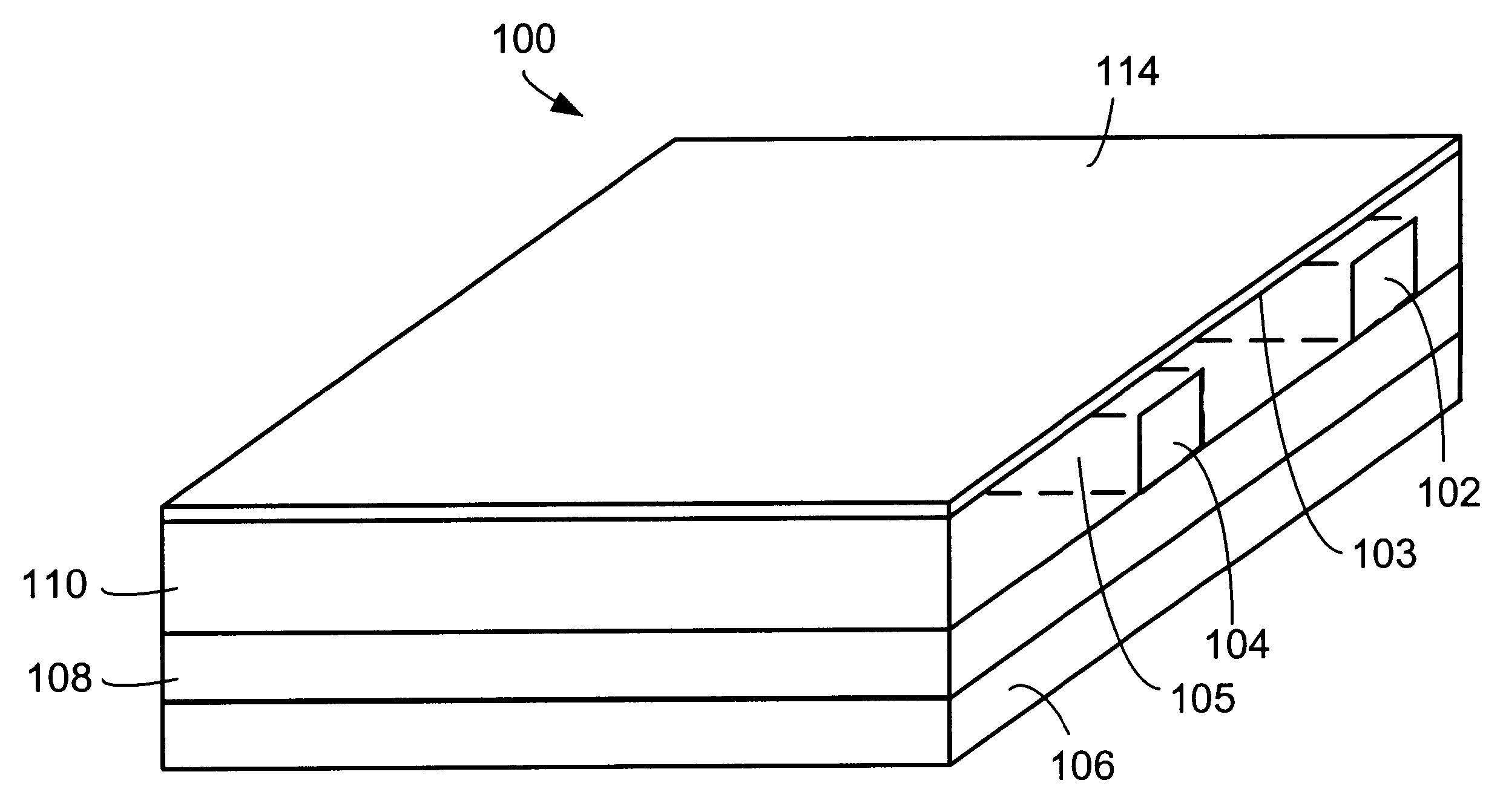
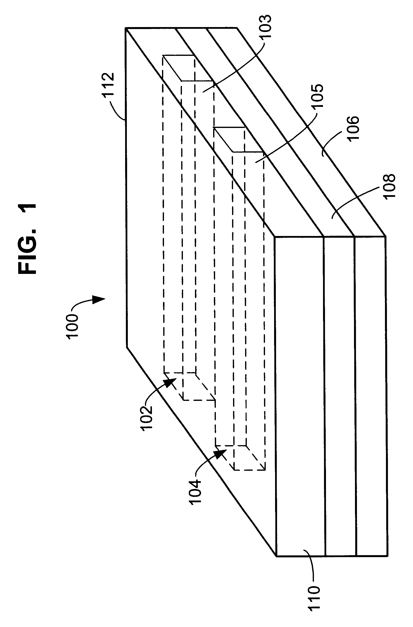
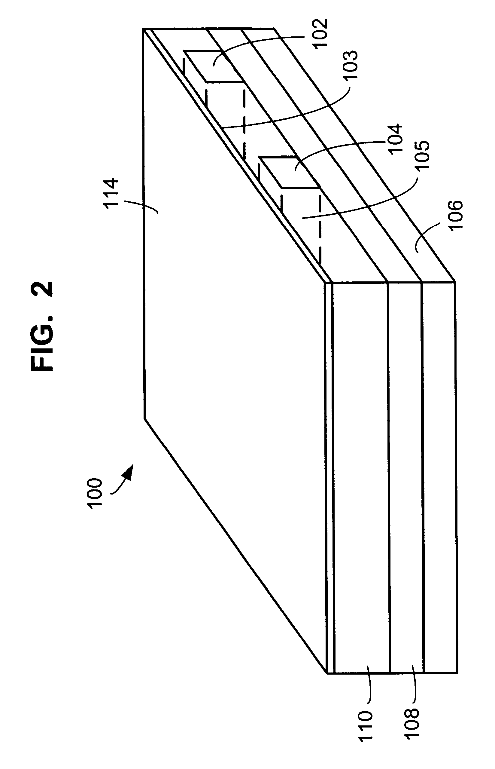
Provided are numerous methods, and structures formed from the same, that address the above-described problems. While preferred examples and numerous alternatives thereto are provided below, it will be appreciated by persons of ordinary skill in the art that these are exemplary in nature. The teachings herein may be used to form a great many optical waveguide devices having Bragg gratings, including optical devices formed by planar lightwave circuit processes and otherwise. Furthermore, while the approaches are described in the context of forming Bragg gratings during an UV exposure process, the teachings herein may be applied to other UV exposure processes in which UV exposure spot size has previously limited the density or close spacing of optical components.

An optical waveguide structure 100 is shown in FIG. 1. The optical structure 100 includes a first waveguide 102 and a second waveguide 104, which are preferably sized for single mode operation, though multi-mode operation is su...


PUM

PropertyMeasurementUnit
Temperatureaaaaaaaaaa
Electrical conductivityaaaaaaaaaa
Electrical resistanceaaaaaaaaaa

Abstract

A method of fabricating a tunable waveguide Bragg grating is provided. The tunable Bragg grating is preferably formed through an ultra-violet (UV) exposure process is preferred. The tunable Bragg grating is formed in an optical substrate, and may be formed in a planar lightwave circuit (PLC). In the latter example, the PLC may include multiple waveguides within close proximity, and the methods described herein provide a way of shielding adjacent waveguides from exposure during the UV exposure process. The Bragg grating is made tunable in one example through a metallic heater layer disposed over a temperature tuned region that is in communication with the Bragg grating for tuning the operation of the Bragg grating in response to changes in a driving signal to the metallic heater.

Description

The present invention relates generally to the fabrication of Bragg gratings and, more specifically, to the fabrication of Bragg gratings in optical waveguides.BACKGROUND OF RELATED ARTIncreasing demands are placed on communication networks as the number of customers grows and as the need to offer more complex services expands. In optical networks, for example, wavelength division multiplexing (WDM) is used to transmit the massive amounts of information passing through the optical network. WDM technology enables information to be transmitted through optical fibers and optical devices in bit streams, each superimposed on light of a different wavelength. A WDM system, for example, may have a single fiber communicating 256 channels, or individual signals, existing at 256 slightly different wavelengths, each channel representing a different user or information stream. To perform routing, switching, multiplexing, demultiplexing, and add / drop functions on these individual signals, wavelen...

Claims


Application Information

Patent Timeline
IPC IPC(8): G02B6/124G02B6/12
CPCG02B6/12004G02B6/124G02F1/3132G02F2201/307G02F1/0147G02B2006/121
Inventor NIKONOV, DMITRI E.
Owner INTEL CORP
Why Eureka
Try Eureka