

Spacer - connector stud for stacked surface laminated multichip modules and methods of manufacture
a technology of spacer and connector stud, which is applied in the direction of solid-state devices, printed circuit structure associations, and semiconductor/solid-state device details, etc., and can solve the problem that the prior art does not disclos
- Summary
- Abstract
- Description
- Claims
- Application Information
AI Technical Summary
Problems solved by technology
Method used
Image

Examples
Embodiment Construction
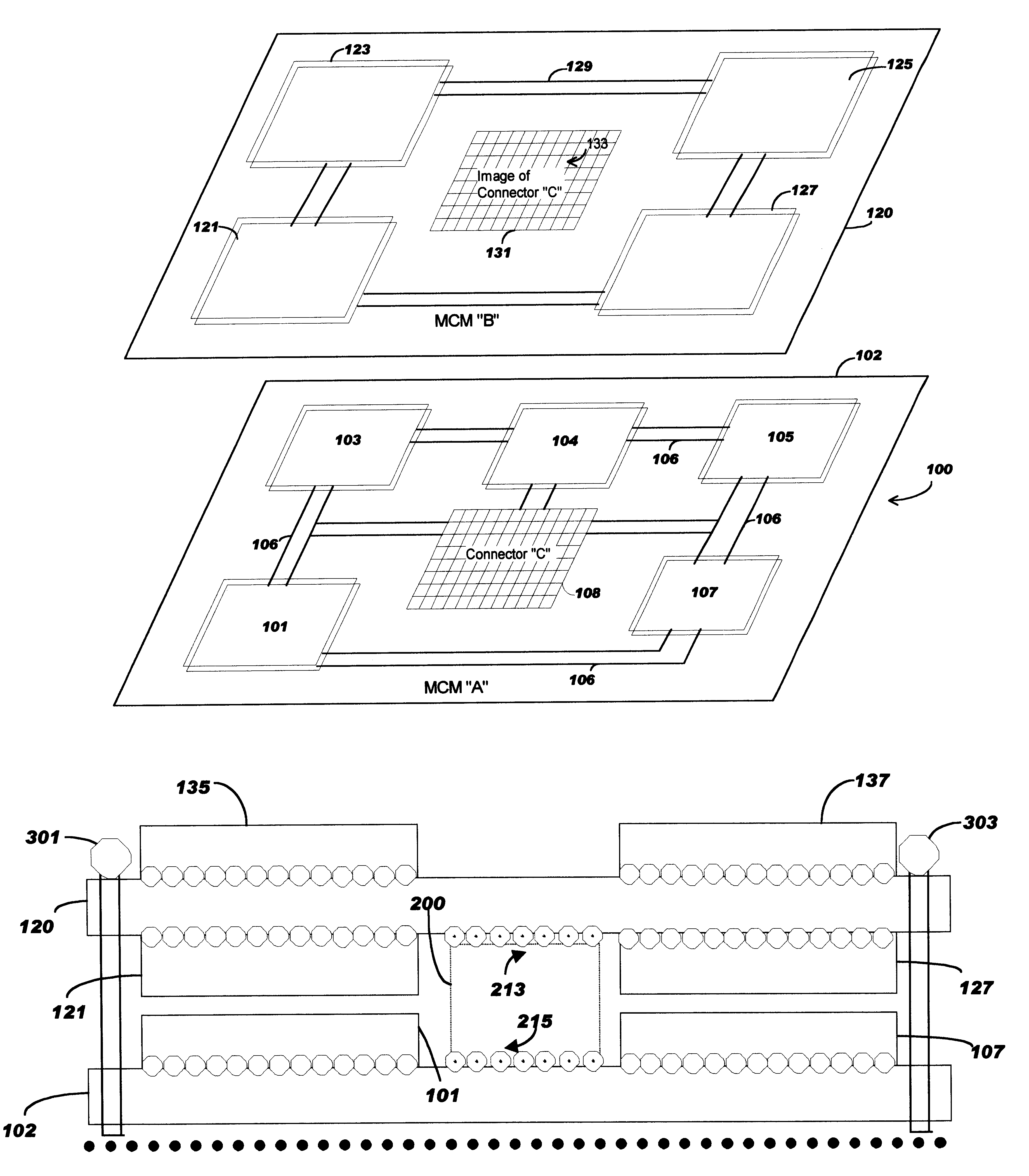
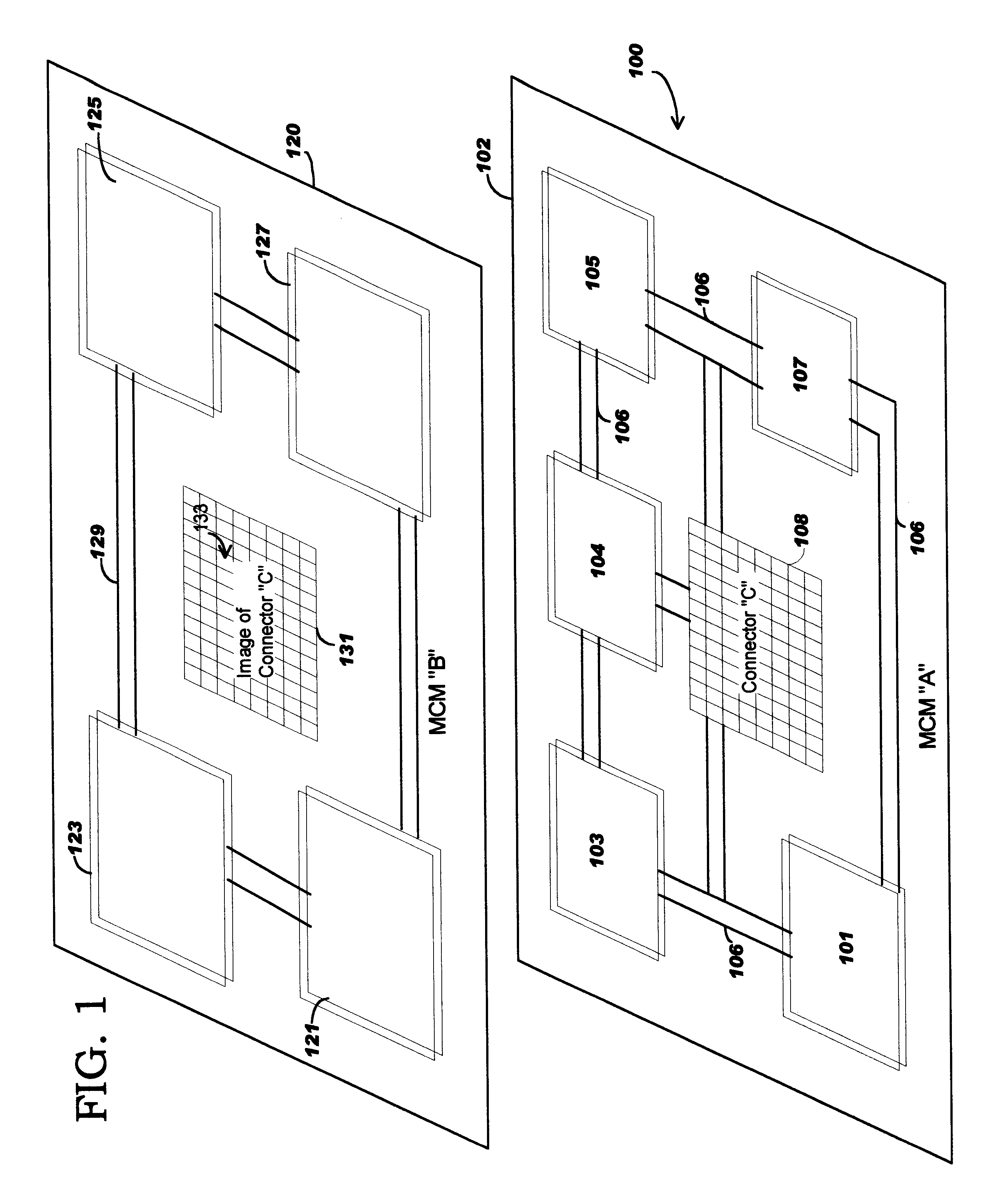
In FIG. 1, a multichip module circuit board 100 comprises a dielectric member 102. In one embodiment, the member is a glass epoxy substrate, covered by a copper layer which is patterned by selective etching to form a wiring layer, including a signal wiring conducting layer 106. A photosensitive thermal setting resin in a solvent is applied to the surface to form an insulating resin layer. The solvent is evaporated from the resin by a pre-cure heating, followed by an exposure and development step to form photo via holes in the board. Thereafter, the resin is cured and the surface of the resin layer is planarized by grinding to provide a flat Surface for subsequent processing as circuitization. The process for forming the substrate is more fully described in U.S. Pat. No. 5,766,825 assigned to the assignee of the present invention and fully incorporated herein by reference.
An assembly of components, 101, 103, 104, 105 and 107 are attached to the circuit board 102, using well-known sur...
PUM
 Abstract
Description
Claims
Application Information