Electrodeposition of metals for forming three-dimensional microstructures

Inactive Publication Date: 2003-04-22
FARADAY TECH INC
View PDF4 Cites 15 Cited by
  • Summary
  • Abstract
  • Description
  • Claims
  • Application Information

AI Technical Summary

Benefits of technology

A further object is to provide an electrochemical method for increasing the height of a free-standing structure on a substrate surface.

Problems solved by technology
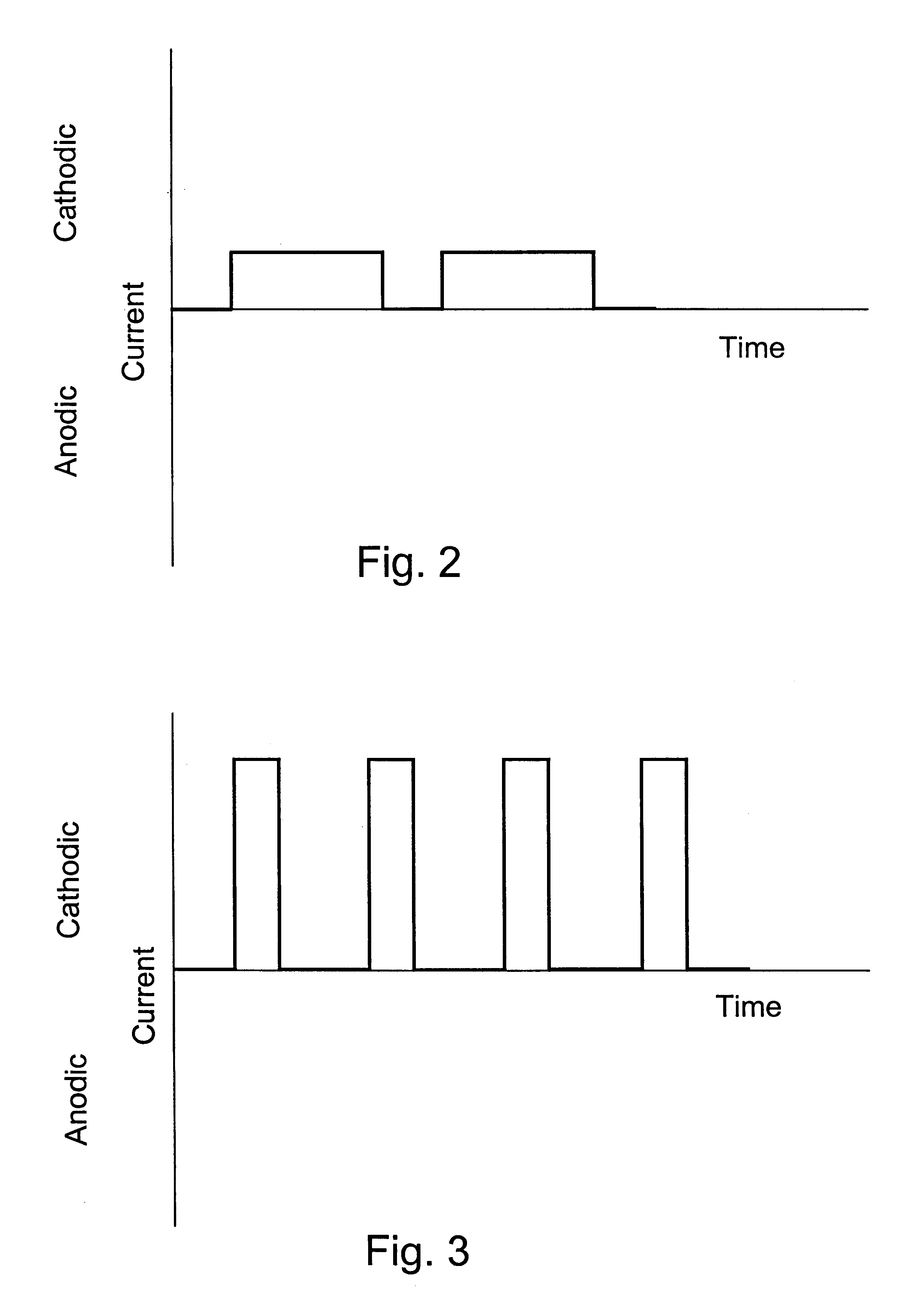
The practical lower limit on the size of such devices is uncertain, but entire devices only a few micrometers across are envisaged.
Evidently, MEMS are not readily capable of being manufactured by conventional machining techniques, which are too coarse for the fabrication and assembly of the miniature and delicate elements that constitute such devices.
However, current techniques involve multiple steps, using many expensive and sometimes hazardous materials, and tend to generate large volumes of waste materials relative to the numbers of devices produced.
As a result of these disadvantages, manufacture of MEMS is currently time-consuming and expensive.
A particular problem encountered in MEMS manufacture, which is not so often experienced in fabrication of semiconductor devices is the need to provide free-standing posts or similar structures extending above a supporting substrate surface.

Method used


Image

  • Electrodeposition of metals for forming three-dimensional microstructures
  • Electrodeposition of metals for forming three-dimensional microstructures
  • Electrodeposition of metals for forming three-dimensional microstructures

Examples


Embodiment Construction

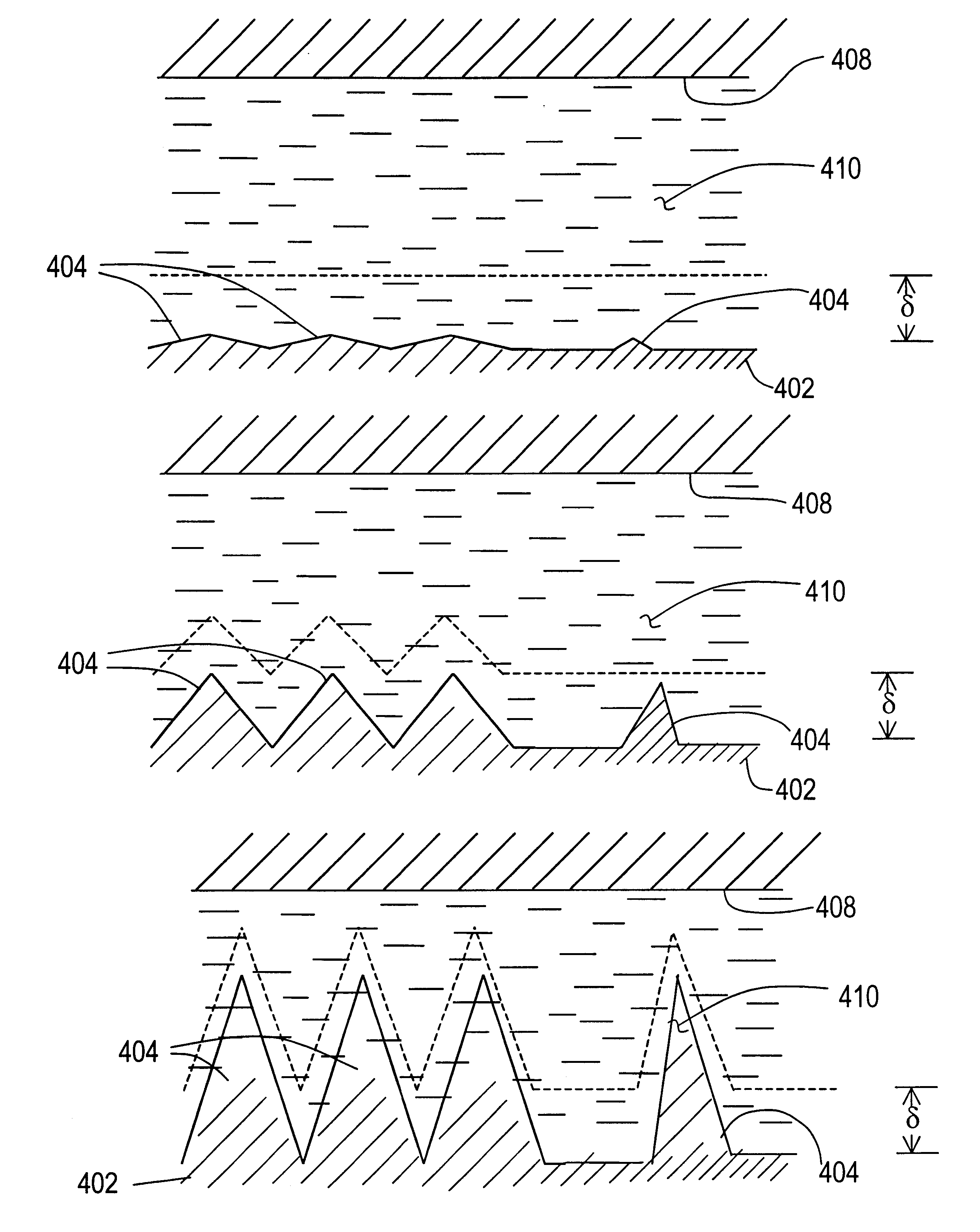
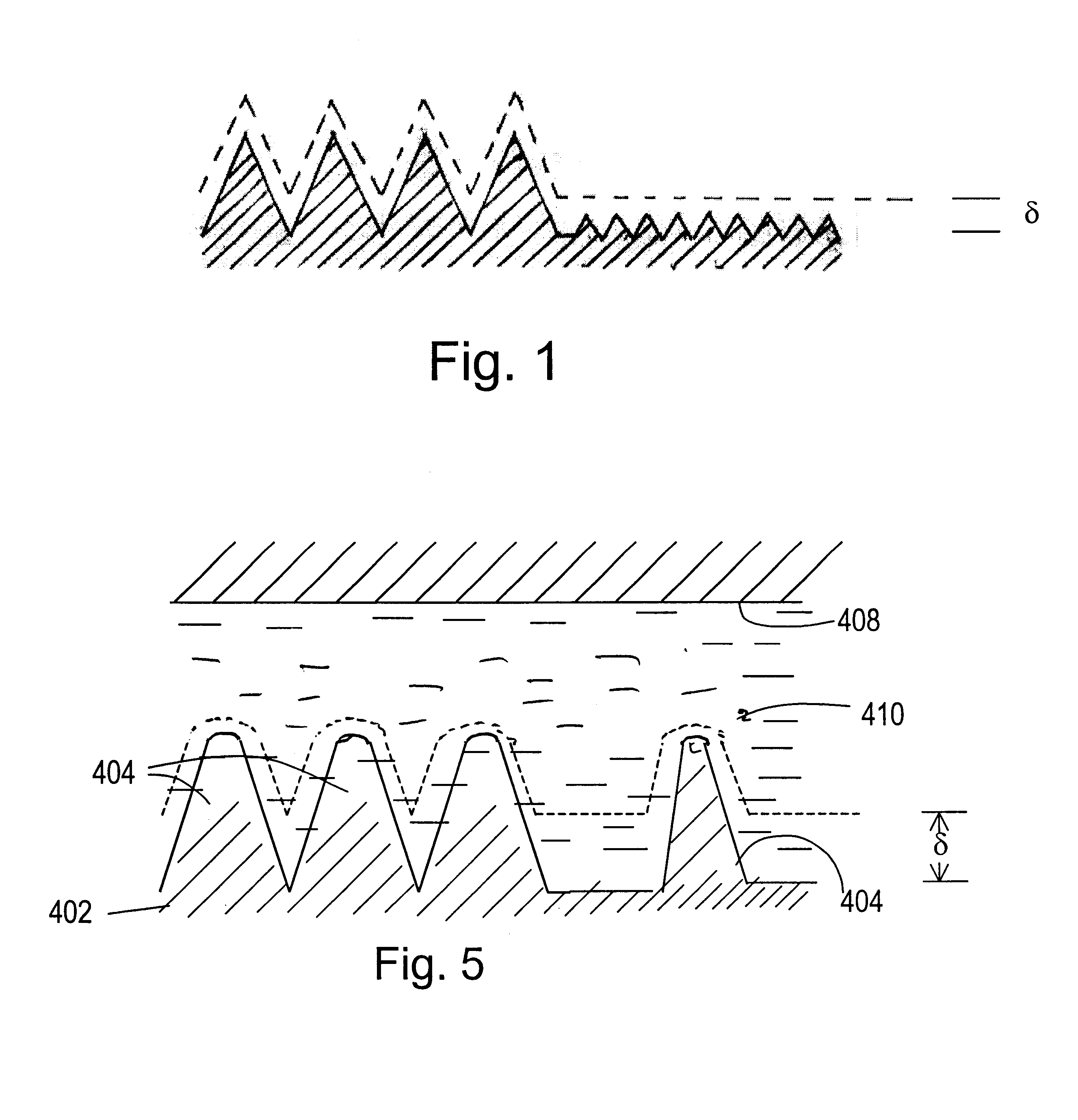
Manufacture of microelectromechanical systems (MEMS) requires the formation, manipulation and assembly of structural elements having sizes of the order of a few millimeters to less than one micrometer. Because such devices have so little mass and often need external power and control, they are typically manufactured or built up while they are secured to a base. Often they are also securely fixed to a supporting substrate in their intended use as well.

The microscopic size of the devices and the elements of which they are made generally precludes conventional means of manufacture. Although micromanipulators exist that can precisely position very small objects, means of joining such objects into an operating machine are as yet poorly developed. Furthermore, individual assembly of such minute devices is unavoidably inefficient. Accordingly, manufacturing means have been adapted from the processes used to fabricate semiconductor devices, as discussed above.

According to the invention free...


PUM

PropertyMeasurementUnit
Fractionaaaaaaaaaa
Fractionaaaaaaaaaa
Fractionaaaaaaaaaa

Abstract

Microscopic mechanical elements suitable for manufacture of microelectromechanical systems (MEMS) are directly prepared by forming a low-relief base of microscopic dimensions on a substrate surface by any conventional means, and electrodepositing a metal preferentially on the upper surface of the base to produce a vertically-extending 3-dimensional structure. In a first step, the patterned substrate and a counterelectrode are contacted with an electrolyte and an electric current is passed between the substrate and counterelectrode, with the substrate being predominantly cathodic with respect the counterelectrode. In a first step the electrolytic environment at the substrate surface is maintained as a microprofile, whereby metal is deposited preferentially at the upper edge or tip of the base until the structure has been increased in height, and, in a second step, the electrolytic environment at the substrate surface is maintained as a macroprofile to continue the deposition of metal at the upper edge or tip of the structure until the desired relief is obtained.

Description

1. Field of the InventionThis invention relates to forming microstructures and more particularly to forming microstructures by electrodeposition.2. Brief Description of the Prior ArtRapid growth in the area of microelectromechanical systems (MEMS) has created a demand for 3-dimensional micron-scale components. Microelectromechanical devices comprise structures of generally conventional shape and function, e.g., beams, posts levers, wheels, and the like, but of a size that is microscopic. Typically, the overall sizes of such devices are no more than a few millimeters in any dimension. The practical lower limit on the size of such devices is uncertain, but entire devices only a few micrometers across are envisaged. As the general name implies, MEMS often incorporate electrical elements as sensors and / or actuators.Evidently, MEMS are not readily capable of being manufactured by conventional machining techniques, which are too coarse for the fabrication and assembly of the miniature and...

Claims


Application Information

Patent Timeline
IPC IPC(8): C25D5/18C25D5/16C25D5/00
CPCC25D5/18C25D5/16C25D5/605
Inventor TAYLOR, E. JENNINGS
Owner FARADAY TECH INC
Why Eureka
Try Eureka