Semiconductor device including gate insulation films having different thicknesses

a technology of semiconductor devices and gate insulation films, which is applied in the direction of semiconductor devices, electrical devices, transistors, etc., can solve the problems of degrading transistor characteristics, affecting the process conditions of forming the thin gate insulation film in the thin film area, and exposing the silicon oxide film formed within the shallow trench to undesired etching

Inactive Publication Date: 2003-04-22
RENESAS ELECTRONICS CORP
View PDF9 Cites 99 Cited by
  • Summary
  • Abstract
  • Description
  • Claims
  • Application Information

AI Technical Summary

Problems solved by technology

In general, a silicon oxide film formed within the shallow trench is subjected to an undesired etching during the etchings performed in the respective areas isolated by the shallow trench.
Once the STI step is formed at the edge portion of the isolation trench, the MOSFETs separated by the shallow trench suffer from an increase in the off-leakage current, whereby transistor characteristics are degraded.
In such a process, however, the process conditions for forming the thin gate insulating film in the thin-film area 27 are inevitably limited by the process conditions for obtaining the final thickness of the thick gate insulating films in the thick-film areas 28 and 29.
The process conditions used for forming the gate insulating films in the later or last step are thus complicated depending on the number of different thicknesses of the gate insulating films in a single LSI.

Method used


Image

  • Semiconductor device including gate insulation films having different thicknesses
  • Semiconductor device including gate insulation films having different thicknesses
  • Semiconductor device including gate insulation films having different thicknesses

Examples


Embodiment Construction

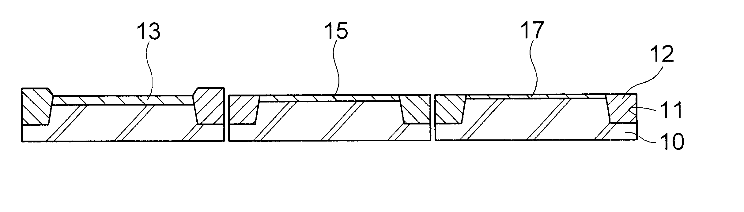
Now, the present invention is more specifically described with reference to accompanying drawings. Referring to FIGS. 2A to 2E, there are shown consecutive steps of a process, according to an embodiment of the present invention, for manufacturing a semiconductor device including an I / O MOS area 60, a low-leakage MOS area 70 and a high-speed MOS area 80. The I / O MOS area 60 includes I / O MOSFETs having a 75-angstrom-thick gate oxide film, the low-leakage MOS area 70 includes low-leakage MOSFETs having a 26-angstrom-thick gate oxide film, and the high-speed MOS area 80 includes high-speed MOSFETs having a 19-angstrom-thick gate oxide film.

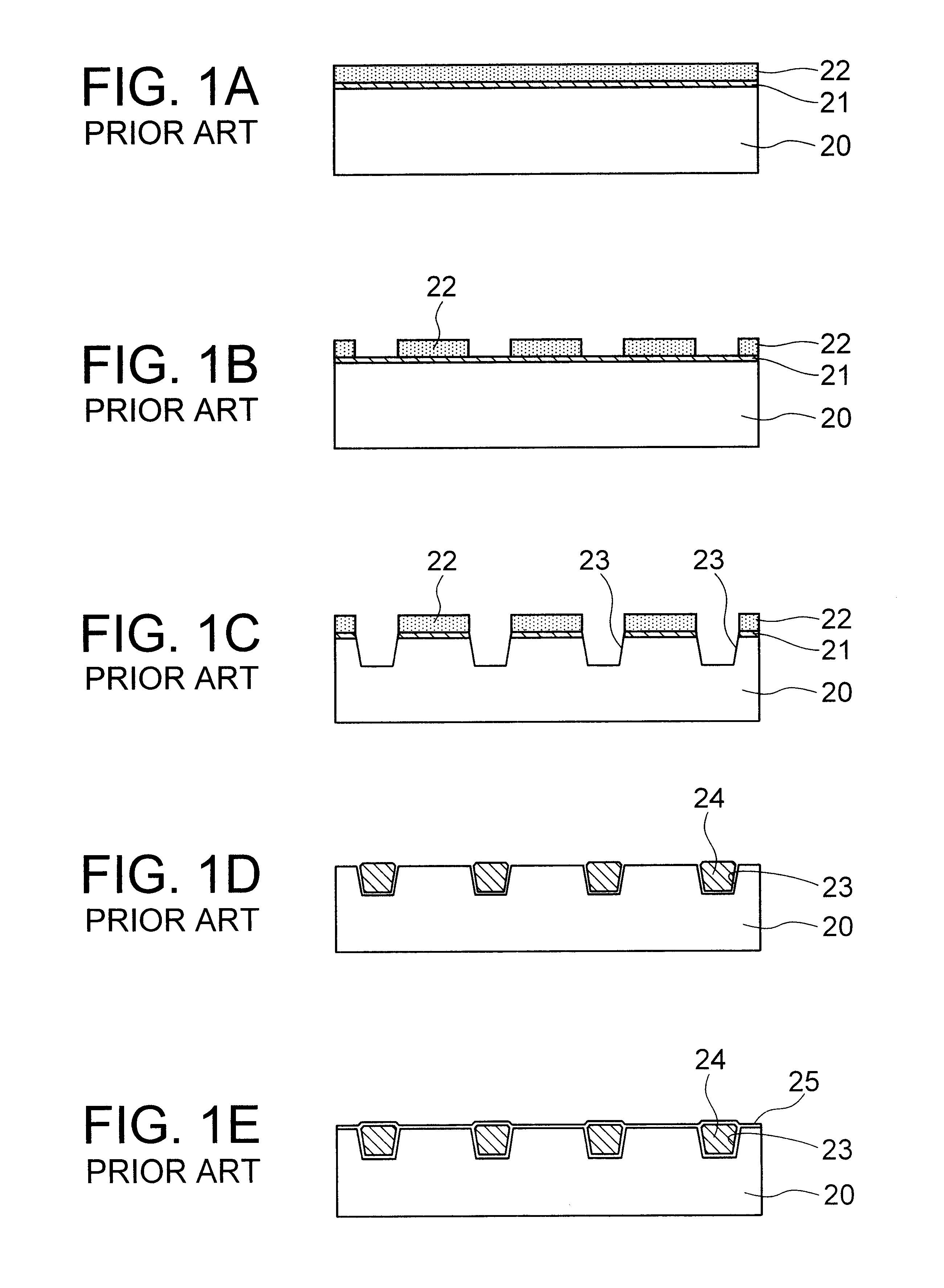
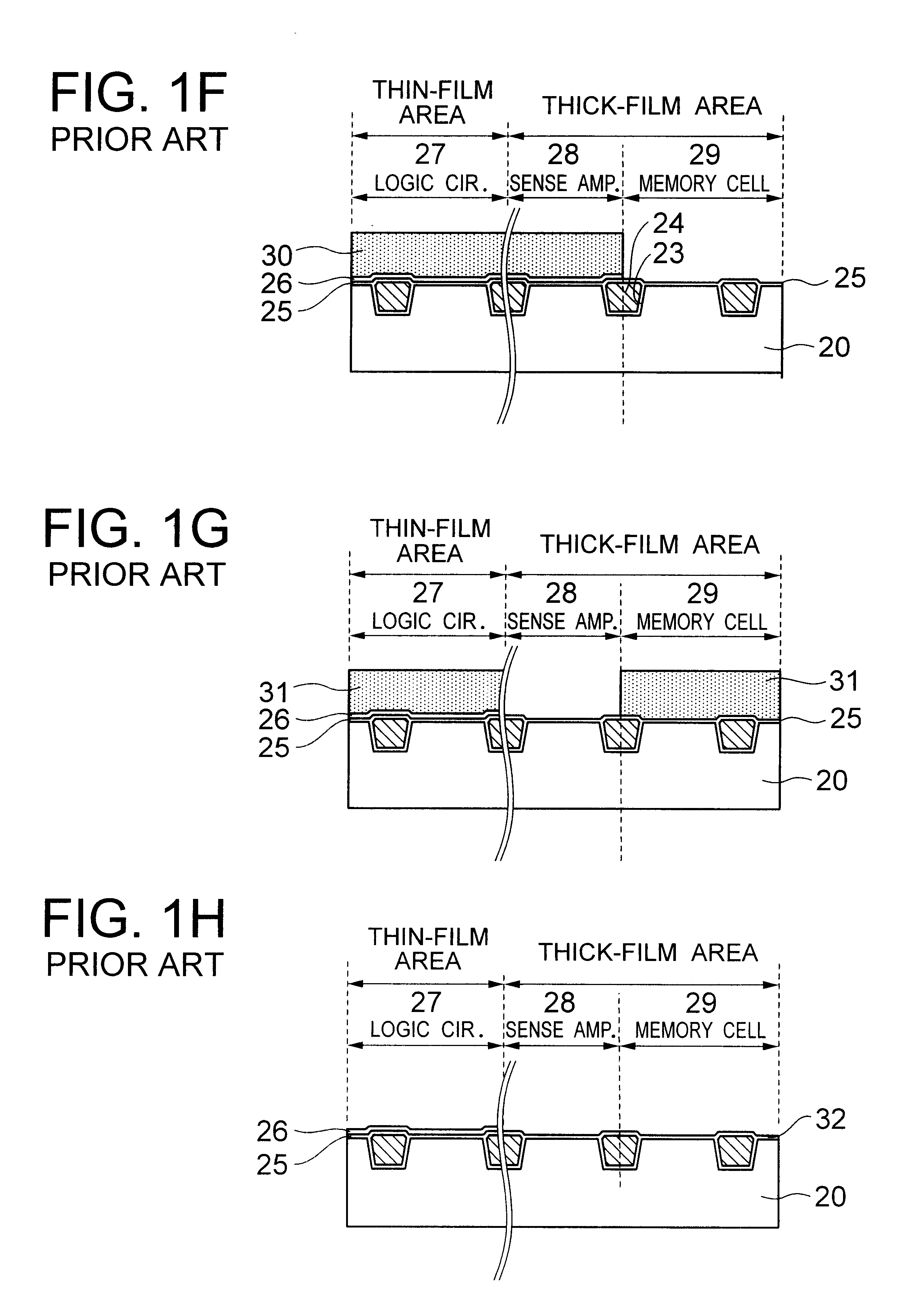
The process of the present embodiment includes initial steps similar to the steps shown in FIGS. 1A to 1D, wherein a shallow trench 11 including an in-trench silicon oxide film 12 is formed on a silicon (semiconductor) substrate 10 to separate the area of the silicon substrate 10 into three MOS areas 60, 70 and 80 each including a large number of tran...


PUM


Abstract

A method for forming three gate oxide films having different thicknesses in first through third circuit areas, respectively. The method includes the consecutive steps of forming a first gate oxide film having a largest thickness in all the areas, removing the first gate oxide film and forming a second gate oxide film having a second largest thickness in the second circuit area, and removing the first gate oxide and forming a third gate oxide film having a smallest thickness in the third circuit area. The resultant gate oxide films have accurate thicknesses.

Description

(a) Field of the InventionThe present invention relates to a semiconductor device including gate insulation films having different thicknesses. The present invention also relates to a method for forming such a semiconductor device.(b) Description of the Related ArtAlong with the developments of finer patterning and high-speed operation of semiconductor devices, a multi-functional semiconductor device, such as a system LSI, formed on a single semiconductor substrate is increasingly used for a variety of applications. In the system LSIs, a finer patterning technology using a STI (shallow trench isolation) structure is generally used. On the other hand, some techniques for the system LSIs use a fabrication process for forming gate insulation films having different film thicknesses for adapting the gate insulation films to different functions of the system LSIs.In a typical STI structure, a problem of the step portion in the STI, known as a STI step problem, is known. The STI step is fo...

Claims


Application Information

Patent Timeline
Patent Type & Authority Patents(United States)
IPC IPC(8): H01L21/70H01L21/8234H01L27/092H01L21/8238H01L27/088H01L27/10
CPCH01L21/823481H01L21/823462
Inventor MASUOKA, SADAAKI
Owner RENESAS ELECTRONICS CORP
Why Eureka
Try Eureka