Integrated antifuse structure for finfet and cmos devices

a finfet and anti-fuse technology, applied in the direction of basic electric elements, semiconductor devices, electrical equipment, etc., can solve the problems of affecting the quality of the device, affecting the performance of the device, and the appearance of the device is not easy to see,

Inactive Publication Date: 2006-06-15
GLOBALFOUNDRIES US INC
View PDF8 Cites 95 Cited by
  • Summary
  • Abstract
  • Description
  • Claims
  • Application Information

AI Technical Summary

Benefits of technology

[0009] It is noteworthy that the antifuse structures fabricated with this process each have a plurality of possible breakdown paths which are electrically in parallel. A conducting path may be formed by...

Problems solved by technology

In the design and manufacture of field-effect transistors (FETs) particularly, it has been found that two features are difficult to scale down: the device current (which is related to the size of the FET gate) and the size of fuse structures.
If devices are formed with shallow-trench isolation (STI), etching of the isolation trench may create sharp corners in the s...

Method used


Image

  • Integrated antifuse structure for finfet and cmos devices
  • Integrated antifuse structure for finfet and cmos devices
  • Integrated antifuse structure for finfet and cmos devices

Examples


Embodiment Construction

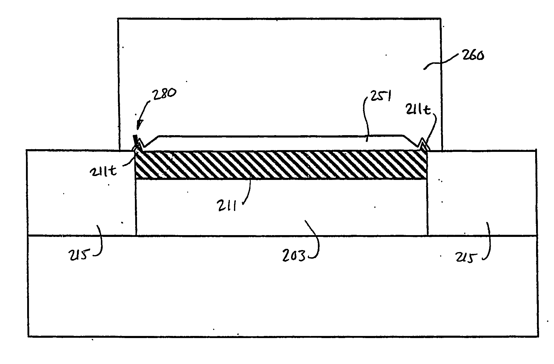
[0014] In accordance with the present invention, a plurality of antifuses is formed at a semiconducting gate structure by oxidation of exposed corners. This process may be applied to either FINFET or planar CMOS gate structures, as detailed below.

(1) Antifuses for FINFET Devices

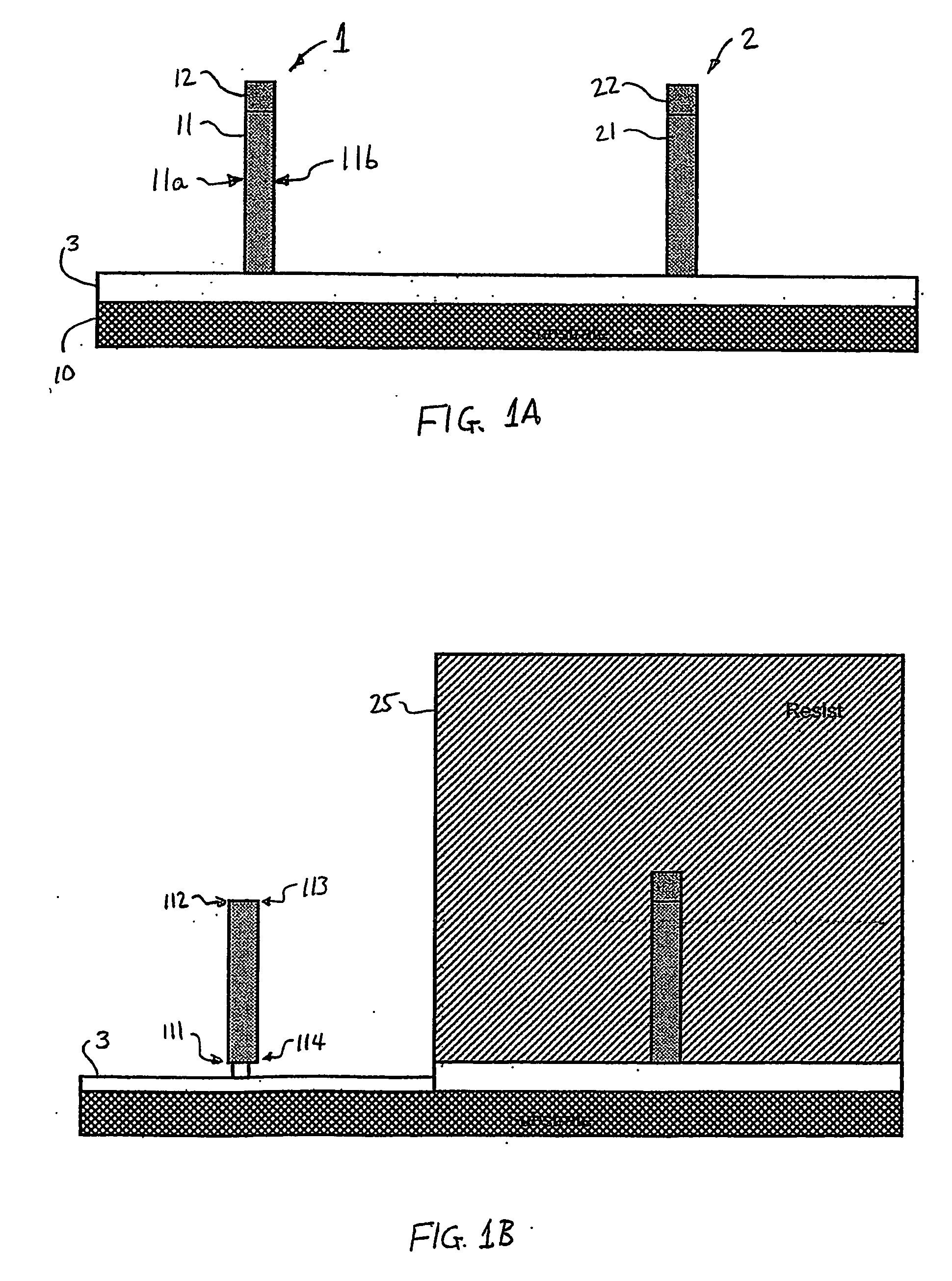
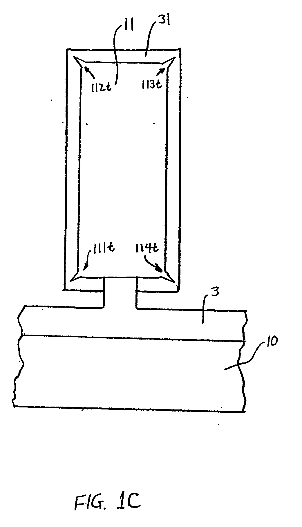
[0015]FIG. 1A shows two neighboring silicon fins 11, 21 which may form the bodies of FINFETs after gate electrode processing. In this illustration, one of these (fin 11) is instead made into an antifuse structure. The fin structure 2, which includes fin 21 and hardmask 22, is coated with a protective layer of resist 25; the resist is exposed and developed to uncover fin structure 1. The exposed portion of the BOX layer 3 is then subjected to an isotropic etch which undercuts silicon fin 11 (see FIG. 1B). The hardmask 12 is also removed in this step. It should be noted that the etching and undercutting results in four exposed corners 111-114 on silicon fin 11.

[0016] The silicon surface of fin 11 is then ox...


PUM


Abstract

A method is described for fabricating and antifuse structure (100) integrated with a semiconductor device such as a FINFET or planar CMOS devise. A region of semiconducting material (11) is provided overlying an insulator (3) disposed on a substrate (10); an etching process exposes a plurality of corners (111-114) in the semiconducting material. The exposed corners are oxidized to form elongated tips (111t-114t) at the corners; the oxide (31) overlying the tips is removed. An oxide layer (51), such as a gate oxide, is then formed on the semiconducting material and overlying the corners; this layer has a reduced thickness at the corners. A layer of conducting material (60) is formed in contact with the oxide layer (51) at the corners, thereby forming a plurality of possible breakdown paths between the semiconducting material and the layer of conducting material through the oxide layer. Applying a voltage, such as a burn-in voltage, to the structure converts at least one of the breakdown paths to a conducting path (103, 280).

Description

TECHNICAL FIELD [0001] This invention relates to the manufacture of very large-scale integrated devices, particularly FINFET and planar CMOS devices, with electrical antifuses integrated therein. BACKGROUND ART [0002] In their ongoing effort to obtain smaller, faster and more efficient semiconductor devices, designers and engineers have attempted to reduce the scale of all the dimensions and features of the devices. In the design and manufacture of field-effect transistors (FETs) particularly, it has been found that two features are difficult to scale down: the device current (which is related to the size of the FET gate) and the size of fuse structures. [0003] To address device scaling limitations in gate design, considerable work has recently been done to develop manufacturable methods to create novel types of gates. One example of a “dual gate” or “wrap-around gate” design is the FINFET device, where the gate oxide is grown on the face of a vertical fin of silicon and the gate is...

Claims


Application Information

Patent Timeline
IPC IPC(8): H01L21/82
CPCH01L21/84H01L27/1203H01L29/785
Inventor RANKIN, JEDHABADEER, WAGDL W.BROWN, JEFFREY S.TONTI, WILLIAM R.
Owner GLOBALFOUNDRIES US INC
Why Eureka
Try Eureka