Semiconductor device

a semiconductor and device technology, applied in the direction of semiconductor devices, basic electric elements, electrical equipment, etc., can solve the problems of insufficient silicon igbt replacement, inability to further improve the performance of trench-gate igbts, loss of carrier injection enhancement effect (ie effect), etc., to achieve small miller capacitance, small switching loss, and small effect of capacitan

Active Publication Date: 2013-02-14
FUJI ELECTRIC CO LTD
View PDF11 Cites 96 Cited by
  • Summary
  • Abstract
  • Description
  • Claims
  • Application Information

AI Technical Summary

Benefits of technology

[0061]According to the invention, a semiconductor device, the Miller capacitance thereof is small, is obtained. According to the invention, a semiconductor device, the ON-voltage thereof is low is obtained. According to the invention, a semiconduct

Problems solved by technology

Therefore, it is difficult to further improve the performances of the trench-gate IGBTs dramatically.
Therefore, the mass-production of compound semiconductor IGBTs enough to replace the silicon IGBTs completely has not been realized yet.
Since it is unrealistic at present to think that t

Method used


Image

  • Semiconductor device
  • Semiconductor device
  • Semiconductor device

Examples


first embodiment

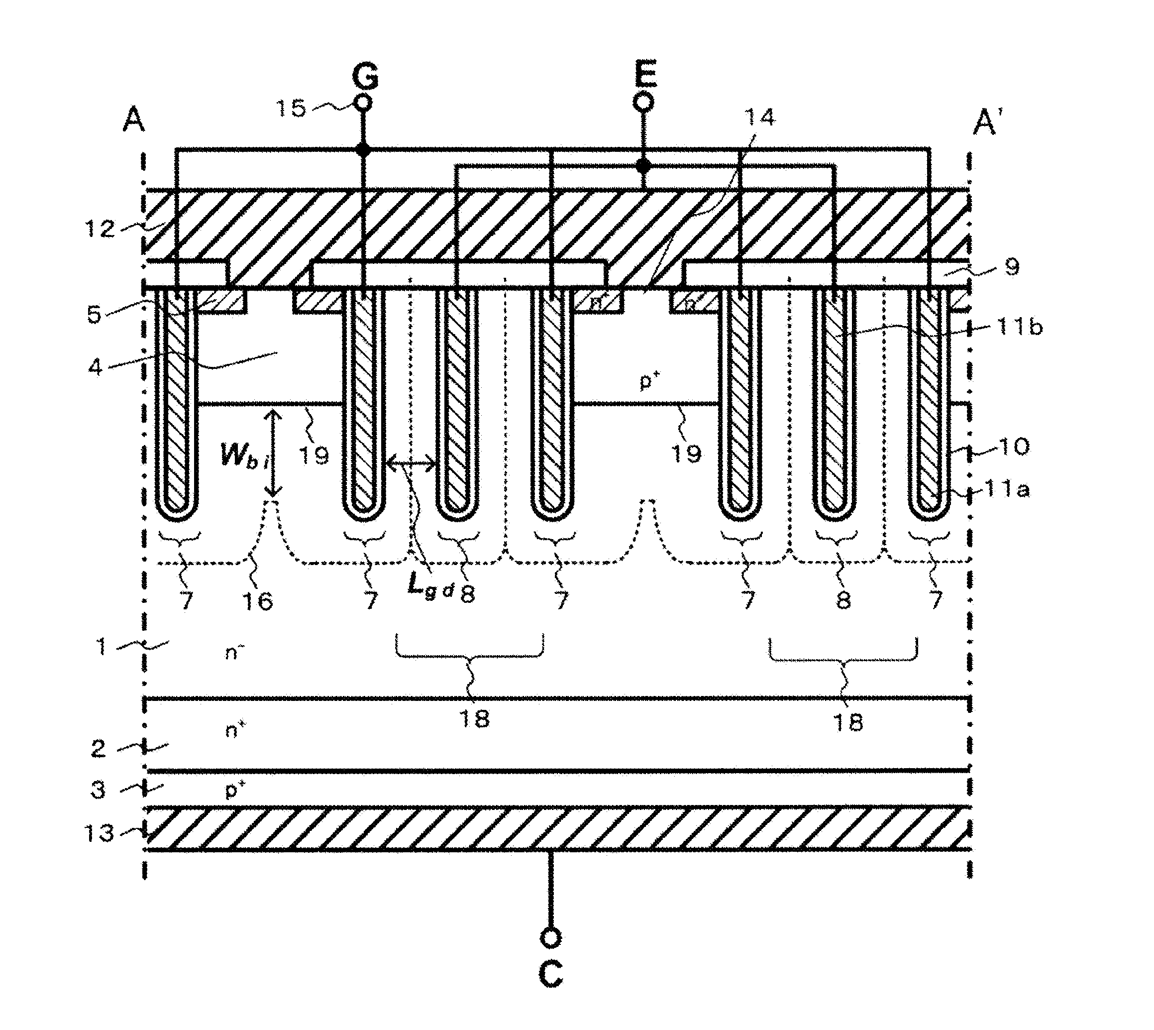
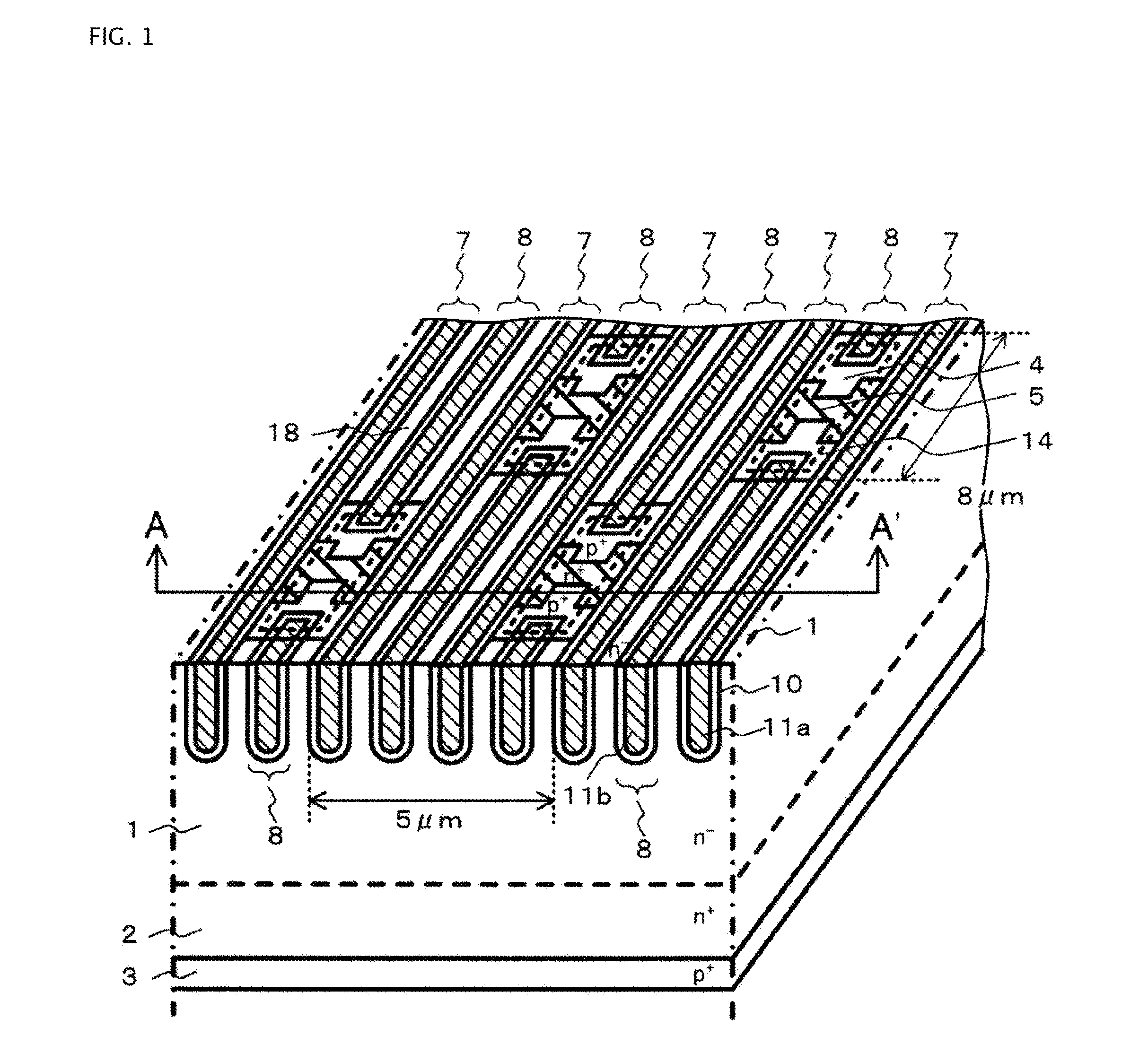
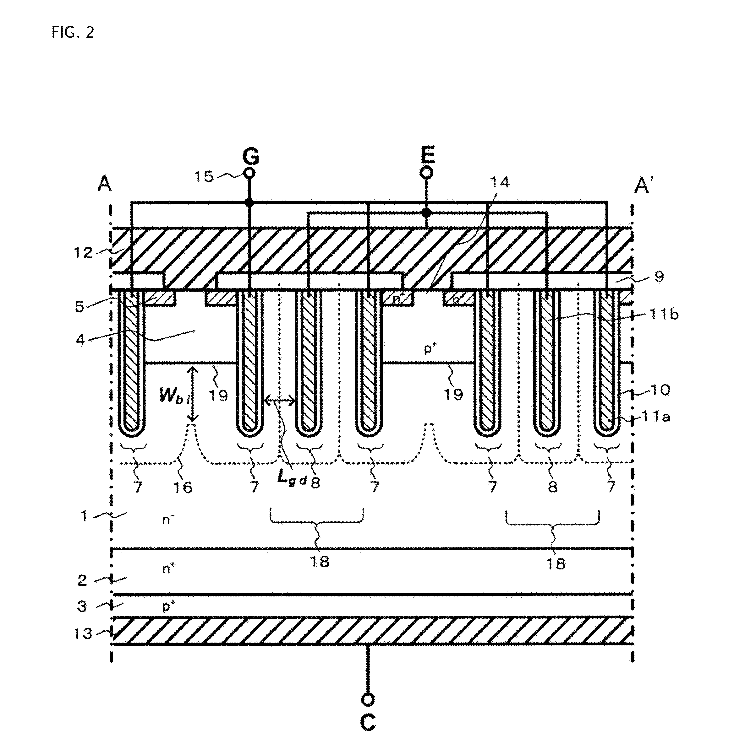
[0098]A semiconductor device according to a first embodiment of the invention will be described below with reference to FIG. 1. FIG. 1 is the oblique view of the semiconductor device according to the first embodiment. In FIG. 1, gate trenches 7 having a stripe planar pattern are formed in one major surface (corresponding to the upper surface in the plane of paper; hereinafter referred to simply as the “upper surface”) of a substrate that works as n-type drift layer 1. On the inner wall of gate trench 7, gate oxide film 10 is formed. Electrically conductive gate polysilicon 11a is formed surrounded by gate oxide film 10.

[0099]In the surface portion on the upper surface side of n-type drift layer 1, p-type base layer 4 in contact with the outer side walls of gate trenches 7 is formed selectively between adjacent gate trenches 7. In other words, p-type base layer 4 is in contact with gate oxide film 10 formed on the inner wall of gate trench 7. In the extending direction of gate trench...

working example 1

[0129]Now the method for manufacturing the semiconductor device according to the invention will be described in detail below in connection with a working example 1. An IGBT of the 600 V class (cf. FIGS. 1 and 2) is obtained according to the first embodiment. First, a silicon wafer (substrate), the specific resistance thereof is 20 Ωcm or higher and 35 Ωcm or lower, is prepared. The specific resistance is set to be 30 Ωcm in the working example 1. Of course, the invention is applicable to the semiconductor devices of the other breakdown voltage classes. The specific resistance is set to be high corresponding to the breakdown voltage class. For example, the specific resistance is set to be 40 Ωcm or higher and 60 Ωcm or lower for the 1200 V class, 60 Ωcm or higher and 90 Ωcm or lower for the 1700 V class, and 100 Ωcm or higher and 250 Ωcm or lower for the 3500 V class. As the breakdown voltage is higher, it is necessary to set the wafer specific resistance to be higher. Therefore, the...

working example 2

[0138]Now the effects according to the first embodiment will be investigated below. Here, the descriptions will be made by comparing the IGBT according to the first embodiment with the conventional IGBT shown in FIG. 32.

[0139]First, an IGBT that includes one dummy trench 8 between adjacent gate trenches 7 (hereinafter referred to sometimes as a “first IGBT”) is fabricated according to the first embodiment. The manufacturing method and the manufacturing conditions are the same with those in the working example 1. For the sake of comparison, an IGBT (conventional IGBT, cf. FIG. 32) that includes no dummy trench 8 between adjacent gate trenches 7 is fabricated. The conventional IGBT is fabricated with the parameters the same with those in the working example 1. The length of p-type base layer 4 in the extending direction of gate trench 7 is set to be 8 μm, the same with that in the working example 1. The spacing between adjacent p-type base layers 4 in the extending direction of gate t...


PUM


Abstract

A semiconductor device includes a stripe-shaped gate trench formed in one major surface of n-type drift layer, a gate trench including gate polysilicon formed therein, and a gate polysilicon connected to a gate electrode. A p-type base layer is formed selectively in mesa region between adjacent gate trenches and a p-type base layer including an n-type emitter layer and connected to emitter electrode. One or more dummy trenches are formed between p-type base layers adjoining to each other in the extending direction of gate trenches. An electrically conductive dummy polysilicon is formed on an inner side wall of dummy trench with a gate oxide film interposed between the dummy polysilicon and dummy trench. The dummy polysilicon is spaced apart from the gate polysilicon and may be connected to the emitter electrode.

Description

FIELD OF THE INVENTION[0001]The present invention relates to semiconductor devices.BACKGROUND[0002]It has been expected eagerly to reduce the electric power consumption in the power semiconductor devices which play a central role in the various uses of electric power converters such as the use for industries and the use for electric vehicles. Among the power semiconductor devices, the use of insulated-gate bipolar transistors (hereinafter referred to as “IGBTs”) has been established firmly, since the IGBTs facilitate obtaining a low ON-voltage by virtue of the conductivity modulation effects thereof and since the IGBTs are controlled easily via the gates thereof driven by a voltage. Especially, the trench-gate IGBT including a gate electrode in a trench formed in a silicon wafer surface facilitates reducing the ON-voltage, since the trench-gate IGBT facilitates increasing the density (total length) of inversion layers (channels).[0003]In the trench-gate IGBTs, the tradeoff performan...

Claims


Application Information

Patent Timeline
IPC IPC(8): H01L29/739
CPCH01L29/0661H01L29/0696H01L29/7397H01L29/41766H01L29/0839H01L29/407H01L29/1095H01L29/41708H01L29/4236
Inventor ONOZAWA, YUICHI
Owner FUJI ELECTRIC CO LTD
Why Eureka
Try Eureka