Semiconductor device and method of manufacturing the same

a technology of semiconductors and semiconductor films, applied in semiconductor devices, electrical devices, transistors, etc., can solve the problems of gate oxide film films with a large film thickness difference, difficult gate oxide film formation,

Inactive Publication Date: 2003-07-01
RENESAS ELECTRONICS CORP
View PDF7 Cites 26 Cited by
  • Summary
  • Abstract
  • Description
  • Claims
  • Application Information

AI Technical Summary

Problems solved by technology

However, the second prior art method has various problems and disadvantages.
For example, gate oxide film films with a large film thickness difference cannot be obtained.
However, when the gate oxide film is thinner than 2.0 nm, it is difficult to form the gate oxide film immediately after the cleaning, because the above-described cleaning forms an oxide film having a thickness of about 1.0 nm (i.e., a natural oxide film or chemical oxide film) on the silicon surface during the cleaning.
This natural oxide film may significantly degrade the reliability of its insulation, because of the low density of

Method used


Image

  • Semiconductor device and method of manufacturing the same
  • Semiconductor device and method of manufacturing the same
  • Semiconductor device and method of manufacturing the same

Examples


Embodiment Construction

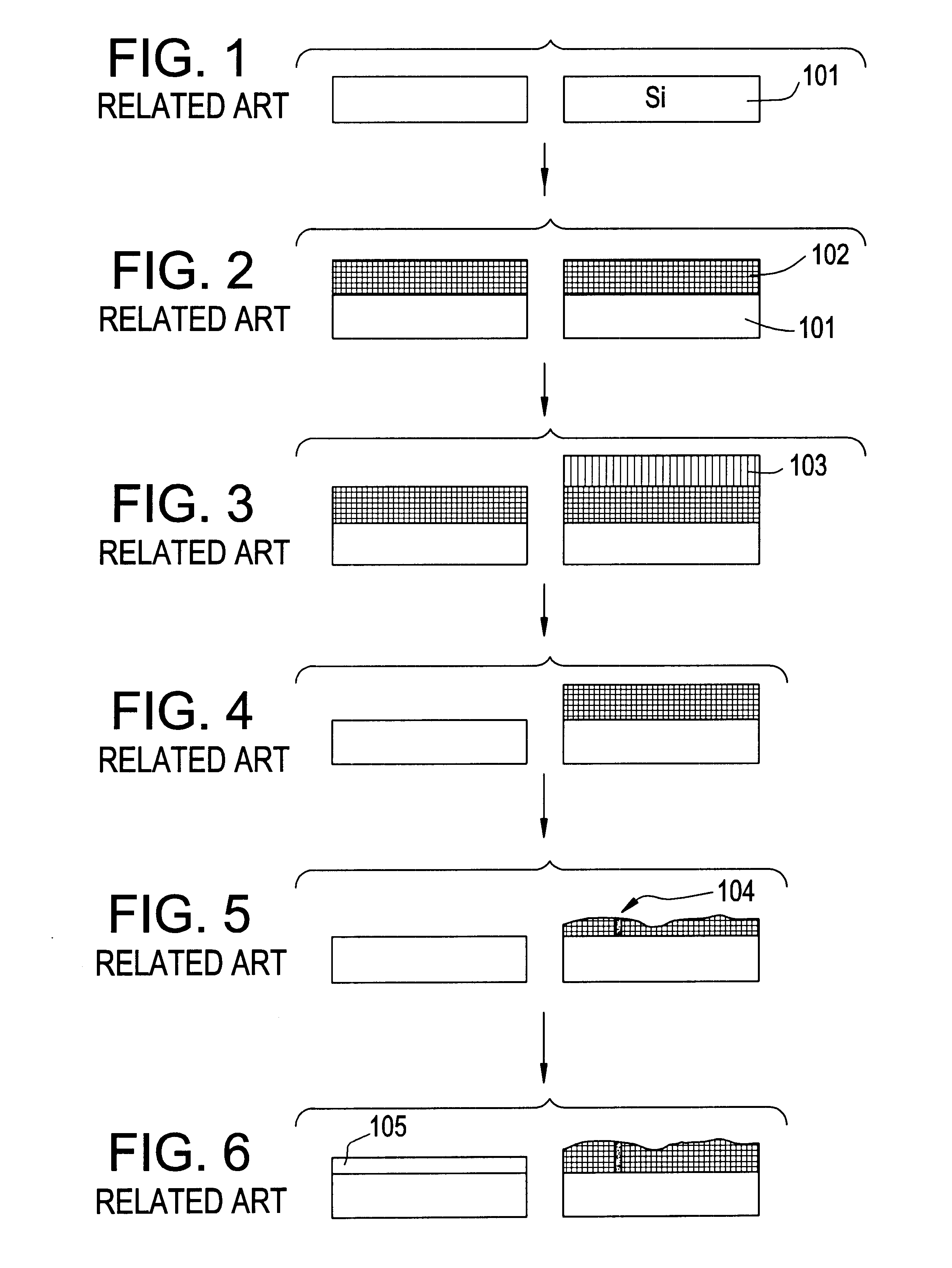
A semiconductor device using the device and manufacturing method according to the preferred embodiments of the present invention will be described with reference to the drawings. It is understood that the invention is not limited to these embodiments, which are provided as only examples of implementations of the invention. For example, the invention is not restricted to gate silicon oxide films, is applicable to other films having different thicknesses from each other.

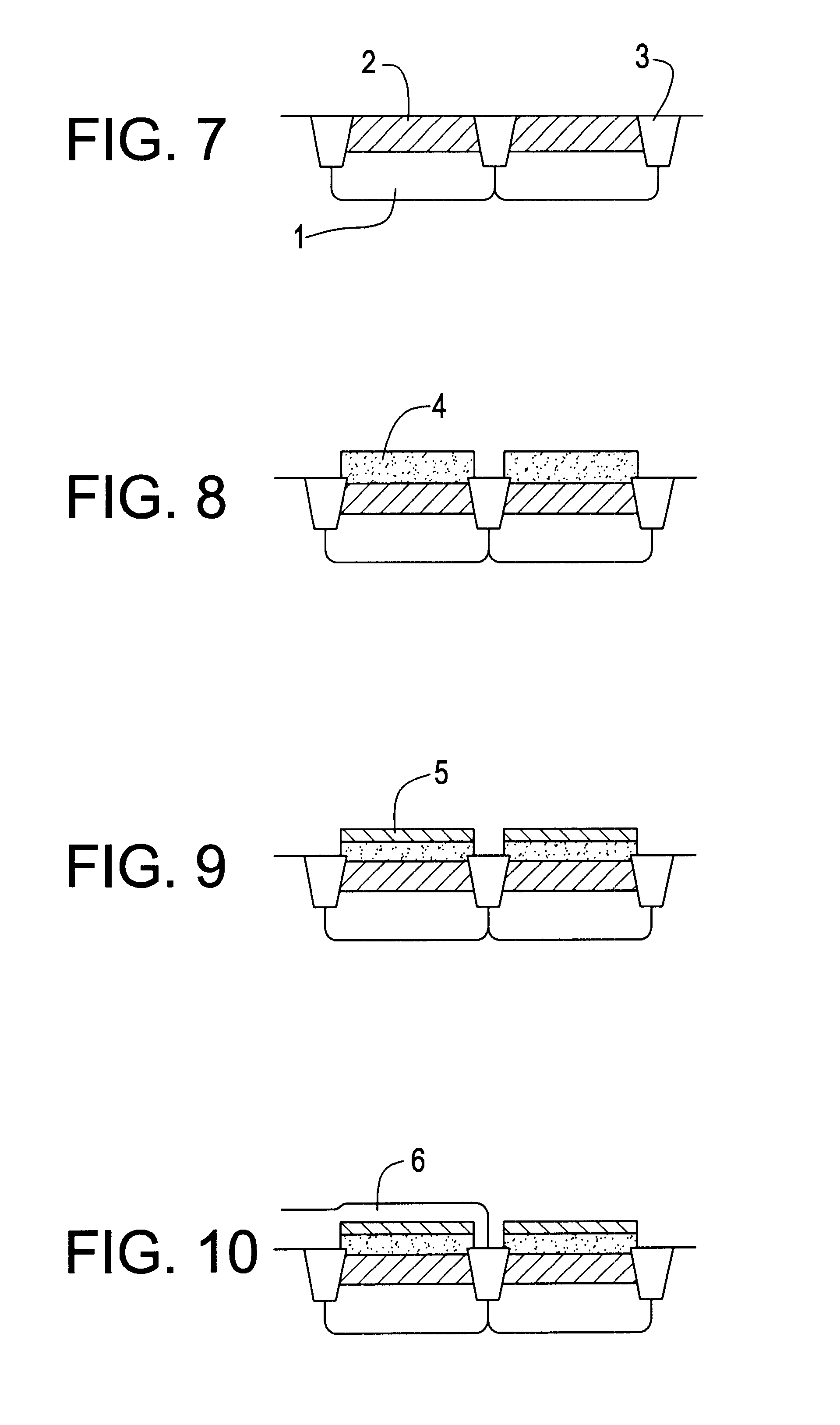
FIGS. 7 to 17 illustrate cross-sectional views showing principal processes according to the first preferred embodiment of the present invention. Other manufacturing methods may be used and the invention is not limited to the manufacturing method described herein. In the first preferred embodiment, gate insulating films with different film thicknesses in adjacent devices in a MOS device will be described. However, the present invention is applicable to gate insulating films in respective regions which are not adjacent t...


PUM


Abstract

To prevent a thick gate oxide film from being damaged by a cleaning and hydrofluoric-acid treatment preprocess performed prior to formation of a thin gate oxide film. A thick first gate oxide film is formed, and an insulating film, having etching resistance against the cleaning and hydrofluoric-acid treatment process for formation of thin second gate oxide film, is formed in an upper region of the first gate oxide film. A resist is then formed in a region where a thick gate insulating film is to be formed, and etching is performed on the first gate oxide film with the resist as a mask. The resist is stripped, then cleaning and hydrofluoric-acid treatment are performed on the silicon surface in a region where a thin gate insulating film is to be formed, and the thin second gate oxide film is formed.

Description

1. Field of the InventionThe present invention relates to a semiconductor device having plural gate insulating films with different film thicknesses, from each other, and a manufacturing method therefor.2. Description of the Related ArtIn the prior art, a method of forming a multioxide device includes forming gate insulating films with different film thicknesses on the same chip. When transistors having different purposes are formed on the same chip, it is necessary to design respective parameters, such as the film thickness of gate oxide film, for each transistor to satisfy performance requirements for each transistor. For example, the film thickness of the gate oxide film must be reduced with reduction of power source voltage in a transistor required to operate at a high speed, while the film thickness of the gate oxide film must be increased with a requirement of comparatively high power source voltage in a transistor used for interface with the outside of the chip.A prior art mu...

Claims


Application Information

Patent Timeline
IPC IPC(8): H01L21/70H01L21/28H01L21/02H01L29/51H01L21/8234H01L21/8238H01L29/40H01L21/311H01L21/316H01L21/314H01L21/306H01L21/318H01L27/088
CPCH01L21/02052H01L21/28202H01L21/28211H01L21/823462H01L21/823857H01L29/513H01L29/518H01L21/31111H01L21/3144H01L21/31604H01L21/3162H01L21/31637H01L21/31641H01L21/31645H01L29/517H01L21/02238H01L21/02255H01L21/0234H01L21/02332H01L21/31116
Inventor HASEGAWA, EIJI
Owner RENESAS ELECTRONICS CORP
Why Eureka
Try Eureka