Solid-state image sensor with reduced smear and noise

a solid-state image sensor and noise reduction technology, applied in the field of solid-state image sensors, can solve problems such as smear and/or nois

Inactive Publication Date: 2003-07-08
NEC ELECTRONICS CORP
View PDF2 Cites 2 Cited by
  • Summary
  • Abstract
  • Description
  • Claims
  • Application Information

AI Technical Summary

Benefits of technology

It is a still further object of the present invention to provide a novel solid-state image sensor, which shows noise-reduced images.
It is yet a further object of the present invention to provide a novel solid-state image sensor, which prevents smear charges generated in a silicon substrate from being drawn to not only a drain region but also a photoelectric converter region.
The potential barrier region prevents charges generated in the semiconductor bulk region from being drawn into the photoelectric converter region. The potential barrier region also prevents leakage of charges from the photoelectric converter region to the semiconductor bulk region. The potential barrier region reduces smear and noise of images.

Problems solved by technology

If charges are injected from the substrate into the drain region, then smear and / or noise may appear on an image sensed by the sensor.

Method used


Image

  • Solid-state image sensor with reduced smear and noise
  • Solid-state image sensor with reduced smear and noise
  • Solid-state image sensor with reduced smear and noise

Examples


first embodiment

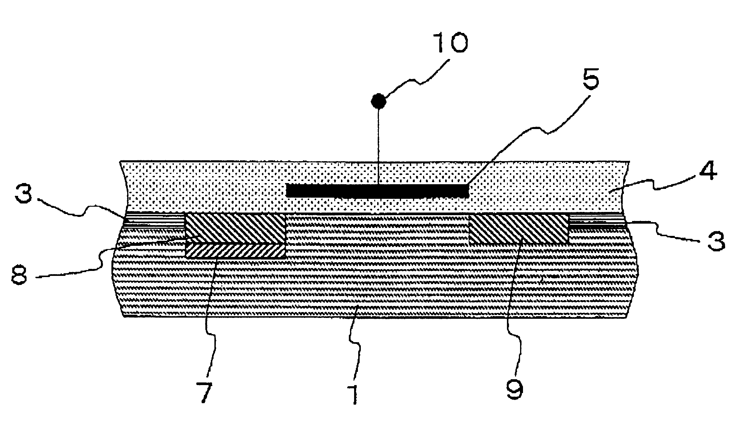
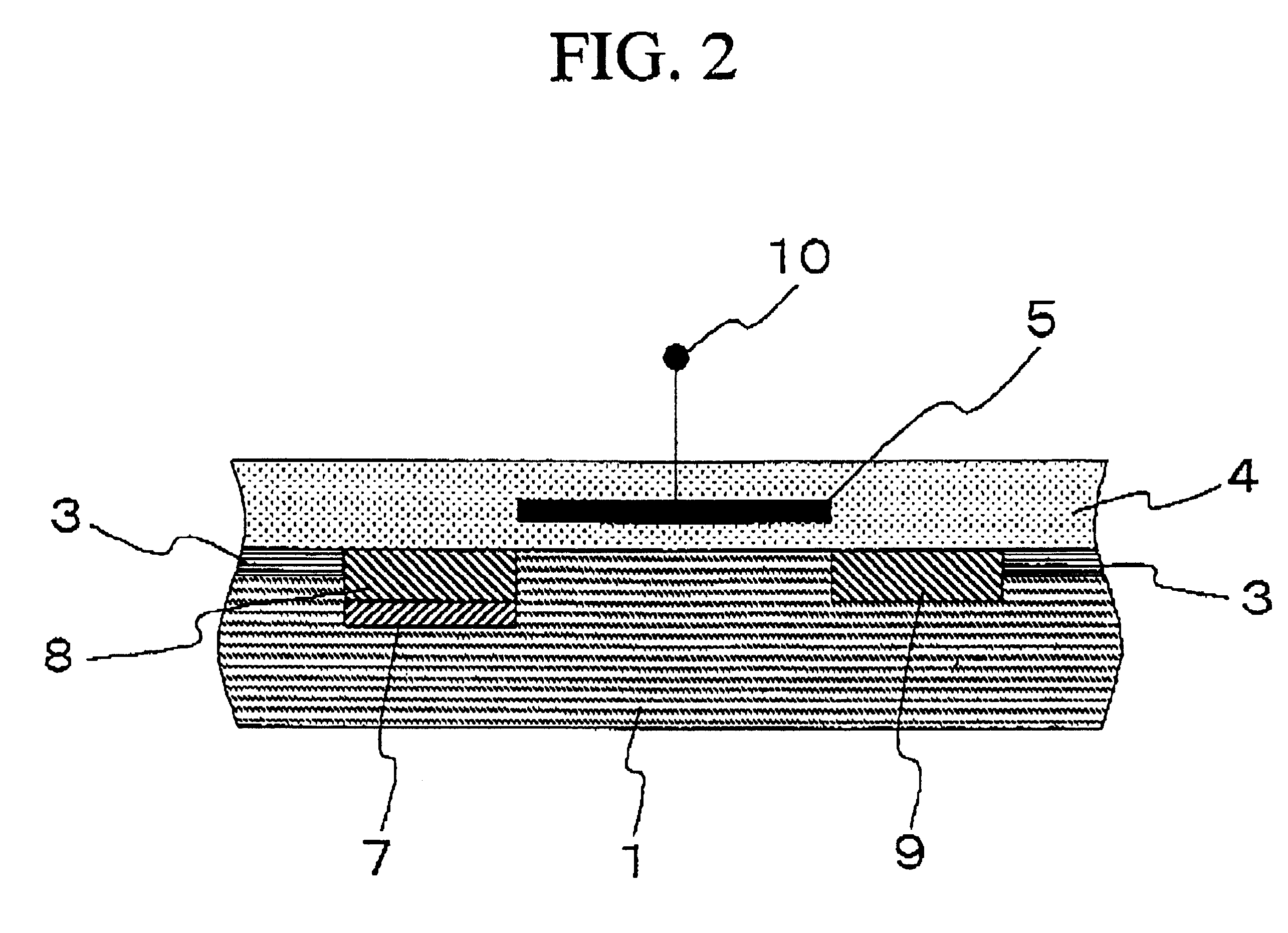
A first embodiment according to the present invention will be described in detail with reference to the drawings. FIG. 2 is a fragmentary cross sectional elevation view of a solid-state image sensor in a first embodiment in accordance with the present invention. The solid-state image sensor has a p-type silicon substrate 1. Isolation regions 3 of silicon dioxide are selectively provided in an upper region of the p-type silicon substrate 1, so that the isolation regions 3 define a device region.

An n-type photoelectric converter region 8 is selectively provided in the device region of the p-type silicon substrate 1. The n-type photoelectric converter region 8 converts incident photons into electric signals. An n-type drain region 9 is also selectively provided in the device region of the p-type silicon substrate 1, wherein the drain region 9 is separated from the n-type photoelectric converter region 8 by a channel region. An insulating layer 4 is provided which overlies an upper face...

second embodiment

A second embodiment according to the present invention will be described in detail with reference to the drawings. FIG. 4 is a fragmentary cross sectional elevation view of a solid-state image sensor in a second embodiment in accordance with the present invention. The solid-state image sensor has a p-type silicon substrate 1. Isolation regions 3 of silicon dioxide are selectively provided in an upper region of the p-type silicon substrate 1, so that the isolation regions 3 define a device region.

An n-type photoelectric converter region 8 is selectively provided in the device region of the p-type silicon substrate 1. The n-type photoelectric converter region 8 converts incident photons into electric signals. An n-type drain region 9 is also selectively provided in the device region of the p-type silicon substrate 1, wherein the drain region 9 is separated from the n-type photoelectric converter region 8 by a channel region. An insulating layer 4 is provided which overlies an upper fa...

third embodiment

A third embodiment according to the present invention will be described in detail with reference to the drawings. FIG. 5 is a fragmentary cross sectional elevation view of a solid-state image sensor in a third embodiment in accordance with the present invention. The solid-state image sensor has a p-type silicon substrate 1. Isolation regions 3 of silicon dioxide are selectively provided in an upper region of the p-type silicon substrate 1, so that the isolation regions 3 define a device region.

An n-type photoelectric converter region 8 is selectively provided in the device region of the p-type silicon substrate 1. The n-type photoelectric converter region 8 converts incident photons into electric signals. An n-type drain region 9 is also selectively provided in the device region of the p-type silicon substrate 1, wherein the drain region 9 is separated from the n-type photoelectric converter region 8 by a channel region. An insulating layer 4 is provided which overlies an upper face...


PUM


Abstract

A solid-state image sensor includes a semiconductor bulk region of a first conductivity type; at least a drain region of a second conductivity type selectively provided in the semiconductor bulk region; at least a photoelectric converter region of the second conductivity type selectively provided in the semiconductor bulk region, and the photoelectric converter region being separated from the drain region; and at least a potential barrier region of the first conductivity type selectively provided in the semiconductor bulk region, the potential barrier region being adjacent to at least a part of bottom and side faces of the photoelectric converter region, and the potential barrier region having a higher impurity concentration than the semiconductor bulk region.

Description

1. Field of the InventionThe present invention relates to a solid-state image sensor, and more particularly to a solid-state image sensor with reduced smear and noise.2. Description of the Related ArtThe solid-state image sensor has a silicon substrate of a first conductivity type. The substrate has a photoelectric converter region of a second conductivity type and a drain region of the second conductivity type. The photoelectric converter region and the drain region are separated by a channel region, which underlies a transfer gate. If charges are injected from the substrate into the drain region, then smear and / or noise may appear on an image sensed by the sensor. In order to have suppressed smear and noise, it was proposed that the photoelectric convener region is deeper in junction depth than the drain region.Japanese laid-open patent publication No. 61-99472 discloses such a proposal as described above. FIG. 1 is a schematic cross sectional elevation view of a conventional soli...

Claims


Application Information

Patent Timeline
Patent Type & Authority Patents(United States)
IPC IPC(8): H01L27/00H01L31/10H01L27/146H04N5/335H04N5/359H04N5/369H04N5/374
CPCH01L27/14601
Inventor NAGATA, TSUYOSHI
Owner NEC ELECTRONICS CORP
Why Eureka
Try Eureka