

Transistor that uses carbon nanotube ring
a carbon nanotube and transistor technology, applied in transistors, solid-state devices, nanoinformatics, etc., can solve the problems of low carrier mobility of silicon, limited switching speed, and many problems in the processing process of silicon devices for further microminiaturization, and near technological limitations
- Summary
- Abstract
- Description
- Claims
- Application Information
AI Technical Summary
Problems solved by technology
Method used
Image

Examples
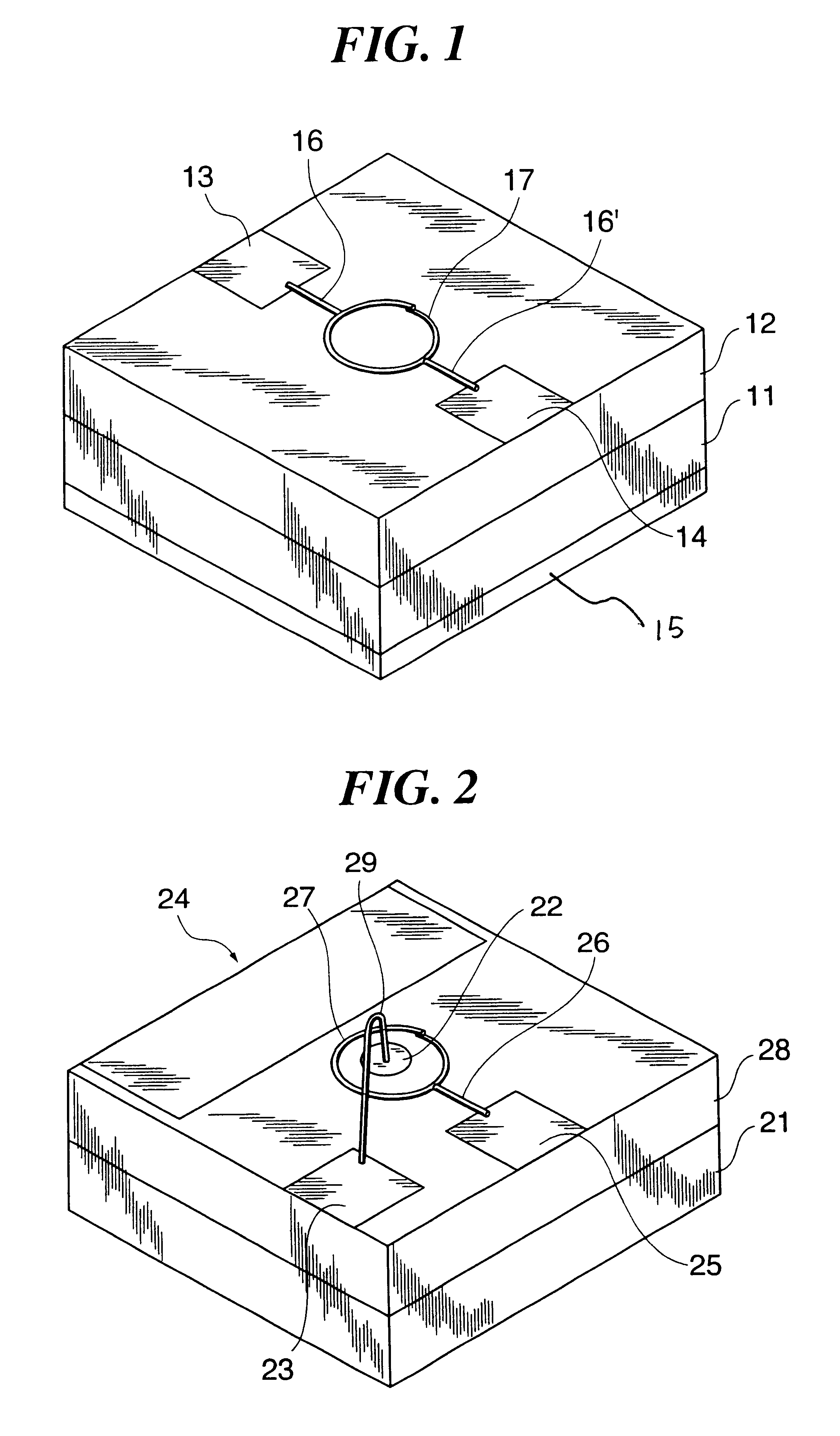
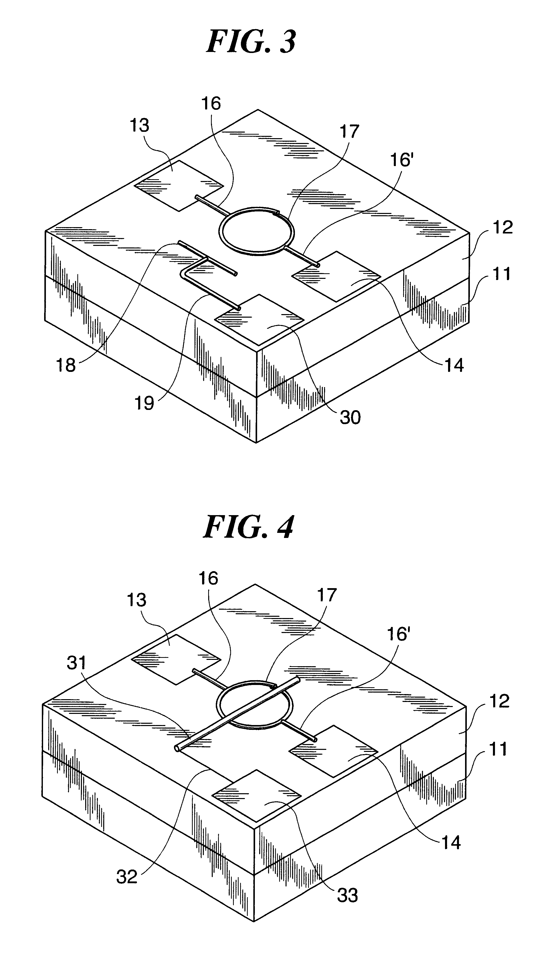
first embodiment example
(First Embodiment Example)
A carbon tube ring was produced by ultrasonically processing a single-wall carbon nanotube produced by the arc discharge method. Specifically, 50 mg of single-wall carbon nanotube was dispersed in 100 ml of methanol solution (surfactant density 5%) of surfactant (Wako Pure Chemical Industries, Ltd., benzalkonium chloride), and ultrasonic processing (frequency 20 kHz, output 50 w) was performed for about one hour. Thereafter, centrifugal separation was performed for about 30 minutes by centrifugation. After the carbon nanotube ring dispersed in the liquid was recovered by a filter, it was cleaned by methanol and acetone on the filter. The ring outside diameter of the obtained carbon nanotube ring was about 20 to 50 nm, and the thickness of the tube part was 2 to 30 nm. In this embodiment example, carbon nanotube rings having p-type semiconductor characteristics that have a ring outside diameter of about 50 nm and a tube part 5 nm in thickness were used.
Using...
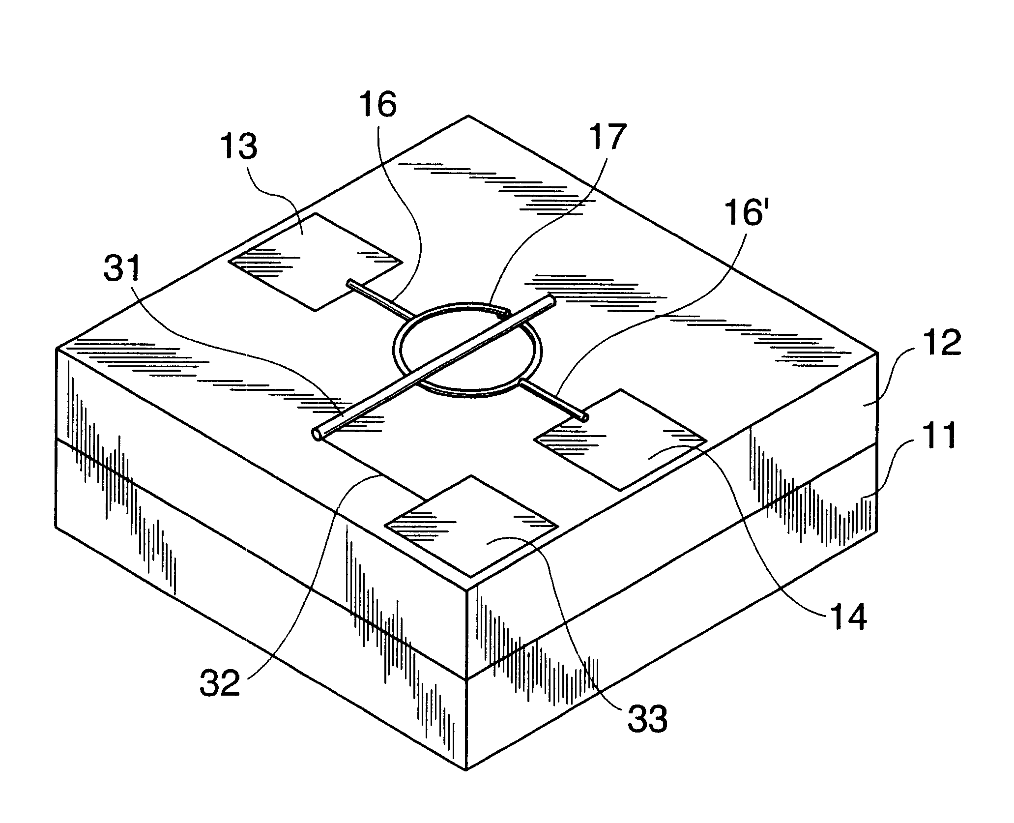
second embodiment example
(Second Embodiment Example)
Using the carbon nanotube rings obtained in the first embodiment example, a transistor shown in FIG. 2 was fabricated.
The same n-type semiconductor substrate 21 of (111) face as in the first embodiment example was provided, and As was implanted to the surface thereof by ion implantation to form the n-type impurity layer 28 of n.sup.+ region. To maximize the density of As on the surface, the surface was polished by about 300 nm by mechanochemical polishing (abrasive GLANZOX).
Next, Au was evaporated on the surface by sputtering and the drain electrode in ohmic contact was formed. Furthermore, as in the first embodiment example, the surface of the n-type semiconductor substrate 21 was subjected to H end processing to stabilize it.
In this state, the above-described carbon nanotube ring dispersed in methanol was expanded on the n-type impurity layer 28 on the surface of the n-type silicon substrate 11 by spin coating, and the carbon nanotube ring 27 was mounted...
PUM
| Property | Measurement | Unit |
|---|---|---|
| diameter | aaaaa | aaaaa |
| diameter | aaaaa | aaaaa |
| diameter | aaaaa | aaaaa |
Abstract
Description
Claims
Application Information