Optical data bus fixing board and optical back plane board

a technology of optical data bus and fixing board, which is applied in the direction of resilient/clamping means, instruments, optical waveguide light guides, etc., can solve the problems of high packaging cost, difficulty in realizing interconnection of multiple nodes, and the inability to fix optical data bus

Inactive Publication Date: 2003-09-16
AICA KOGYO CO LTD +1
View PDF8 Cites 4 Cited by
  • Summary
  • Abstract
  • Description
  • Claims
  • Application Information

AI Technical Summary

Problems solved by technology

However, when optical interconnection utilizing optical fibers as a signal transmission medium is introduced not only into systems for industrial use but also into systems commonly used in offices and homes, there are problems, such as high packaging cost due to need for accurate positioning of optical connections and difficulty in realizing interconnection of multiple nodes with a simple structure.
The use of the above described optical data bus as a signal transmission medium, however, presents problems of how to fix the optical data bus.
However, there has not been provided any appropriate fixing means in order to use, as a signal transmission medium, an optical data bus having a step-wise configuration, as shown in FIGS. 6A to 6C.
In this case, however, the unevenness is attenuated by the use of the adhesive and light cannot be reflected and diffused such that desired characteristics are obtained.
The flat plate may be made of metal, but preferably is made of resin instead of metal because the difference of thermal expansion coefficient between a metal plate and the optical data bus is relatively large compared with a resin plate and therefore a metal plate is prone to damage the optical data bus.
However, when the configuration of the recess for insertion of an optical data bus is larger than the configuration of the optical data bus, it becomes difficult to properly position the optical data bus (i.e. respective signal light incoming / outgoing areas) on the flat plate (i.e. the optical data bus fixing board).

Method used


Image

  • Optical data bus fixing board and optical back plane board
  • Optical data bus fixing board and optical back plane board
  • Optical data bus fixing board and optical back plane board

Examples


Embodiment Construction

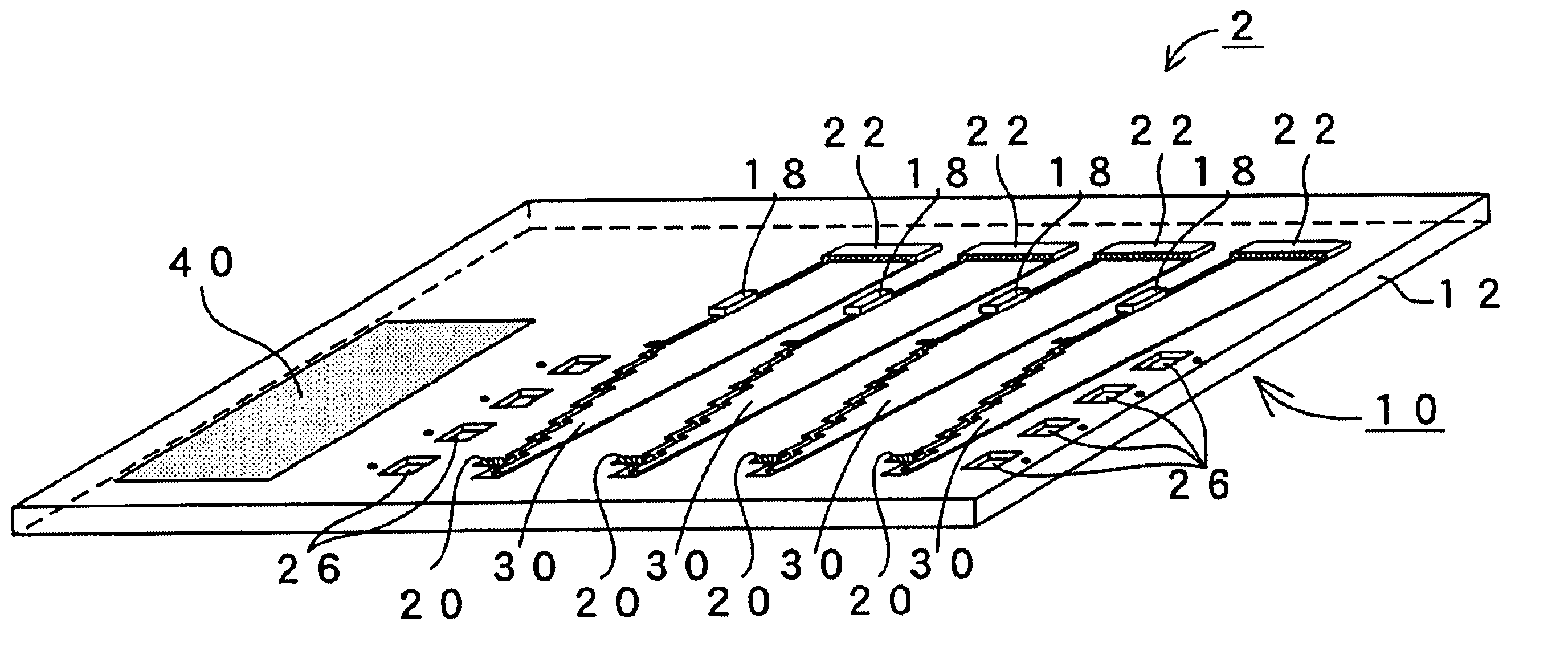
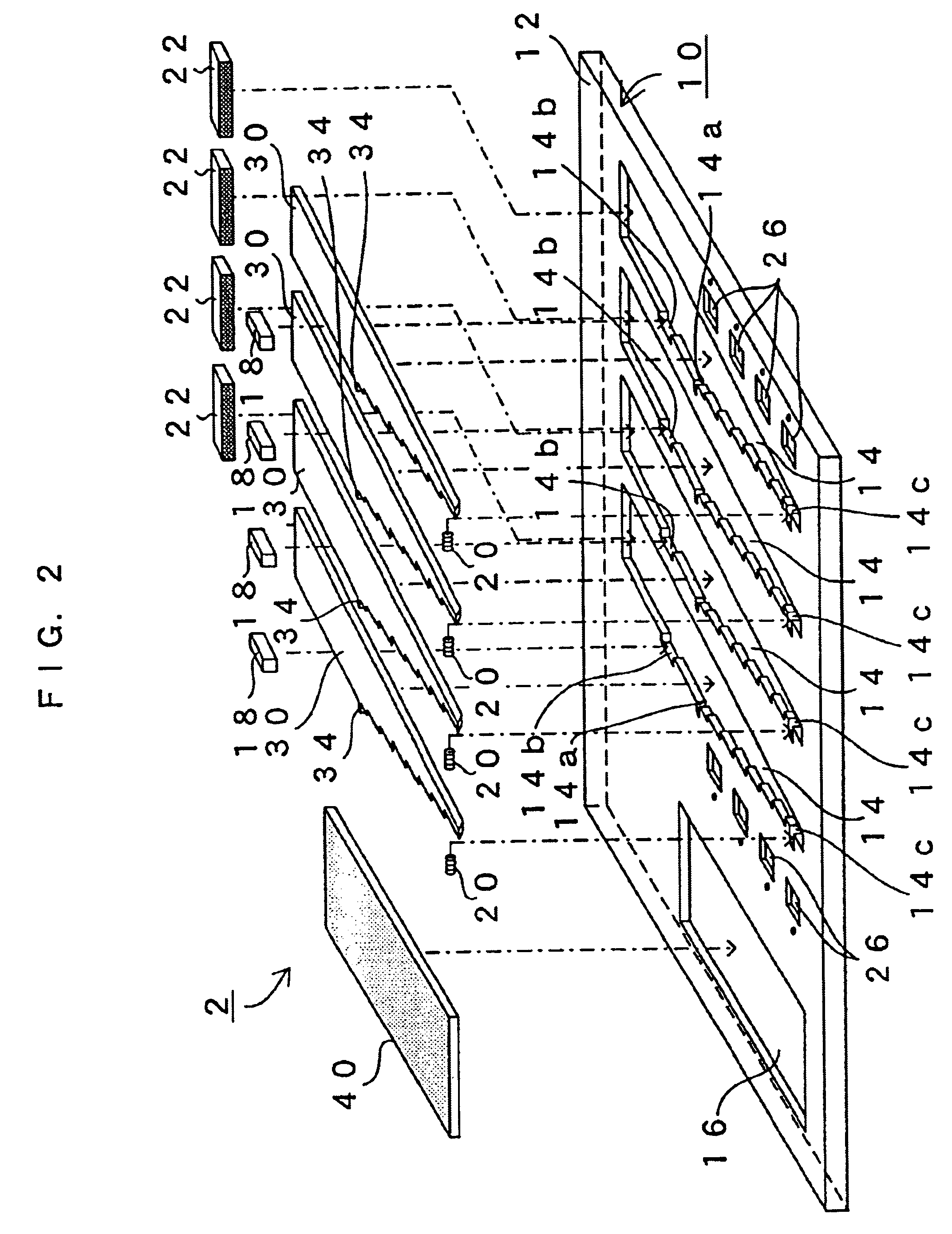
As shown in FIGS. 1 trough 3, an optical back plane board 2 in the present embodiment comprises an optical data bus fixing board 10, including a flat plate 12 of synthetic resin, a plurality of optical data buses 30 fixed, respectively, within a plurality of (e.g. four (4) in the present embodiment) recesses for insertion of an optical data bus 14, and a printed circuit board 40 fixed within a recess for insertion of a printed circuit board 16 (see FIG. 2). On the printed circuit board 40, where a power supply line and an electrical signal transmission line are provided, electronic components for processing signals are mounted if required. The configuration or assembly method of the printed circuit board 40, however, will not be discussed herein since the printed circuit board 40 does not constitute a particular feature of the present invention.

As shown in FIGS. 4A and 4B, the optical data bus 30 has basically the sane structure as an optical data bus 50 shown in FIGS. 6A through 6C...


PUM


Abstract

An optical data bus fixing board suitable for using an optical data bus as a signal transmission medium and an optical back plane board. A recess for inserting an optical data bus, which is made of a rectangular light transmissive resin substrate and comprises a step-wise side along the longitudinal direction and signal light incoming / outgoing areas formed by sloping the longitudinal end of each step at 45 degrees in relation to the substrate surface, is formed in the surface of a flat plate in order to easily and efficiently use the optical data bus as a signal transmission medium for interconnecting various signal processing circuits. The optical data bus is inserted and fixed within the recess by being pressed and biased from the back end by a first holding member including a reflective diffusion plate and from the side by a second holding member including a flat spring.

Description

(i) Field of the InventionThe present invention relates to a fixing board for fixing an optical data bus comprising a long plate of a light transmissive material having one side formed into a step-wise configuration and signal light incoming / outgoing areas formed by sloping each end surface of each step approximately at 45 degrees in relation to the plate surface, and relates to an optical back plane board using the fixing board.(ii) Description of the Related ArtTo improve the processing performance of a signal processing unit, which employs a parallel architecture comprising a back plane board (mother board) and a plurality of nodes (daughter board), enhancement of the bandwidth by increasing the speed of transmission through a bus and bit multiplication has been sought.Although further speed increase is required for such a signal processing unit employing a parallel architecture, the achievement of further speed increases using a conventional electrical wiring requires a circuit ...

Claims


Application Information

Patent Timeline
Patent Type & Authority Patents(United States)
IPC IPC(8): G02B6/43G02B6/28H05K7/12
CPCG02B6/43
Inventor KATO, MAKOTOITO, SHOJITANAKA, AKIHIROHIGASHIURA, KENICHI
Owner AICA KOGYO CO LTD
Why Eureka
Try Eureka