

Stacked chip scale package structure
a technology of stacking and chip scale, applied in the direction of semiconductor devices, electrical equipment, semiconductor/solid-state device details, etc., can solve the problems of die cracking, inability to adjust the direction of the upper chip, and inability to use the chip design widely
- Summary
- Abstract
- Description
- Claims
- Application Information
AI Technical Summary
Benefits of technology
Problems solved by technology
Method used
Image

Examples
Embodiment Construction
The present invention is characterized in that dummy dies are disposed below the suspended portion of an upper chip as a support during wire bonding to resolve the problem of die crack caused by wire bonding of suspended chip.
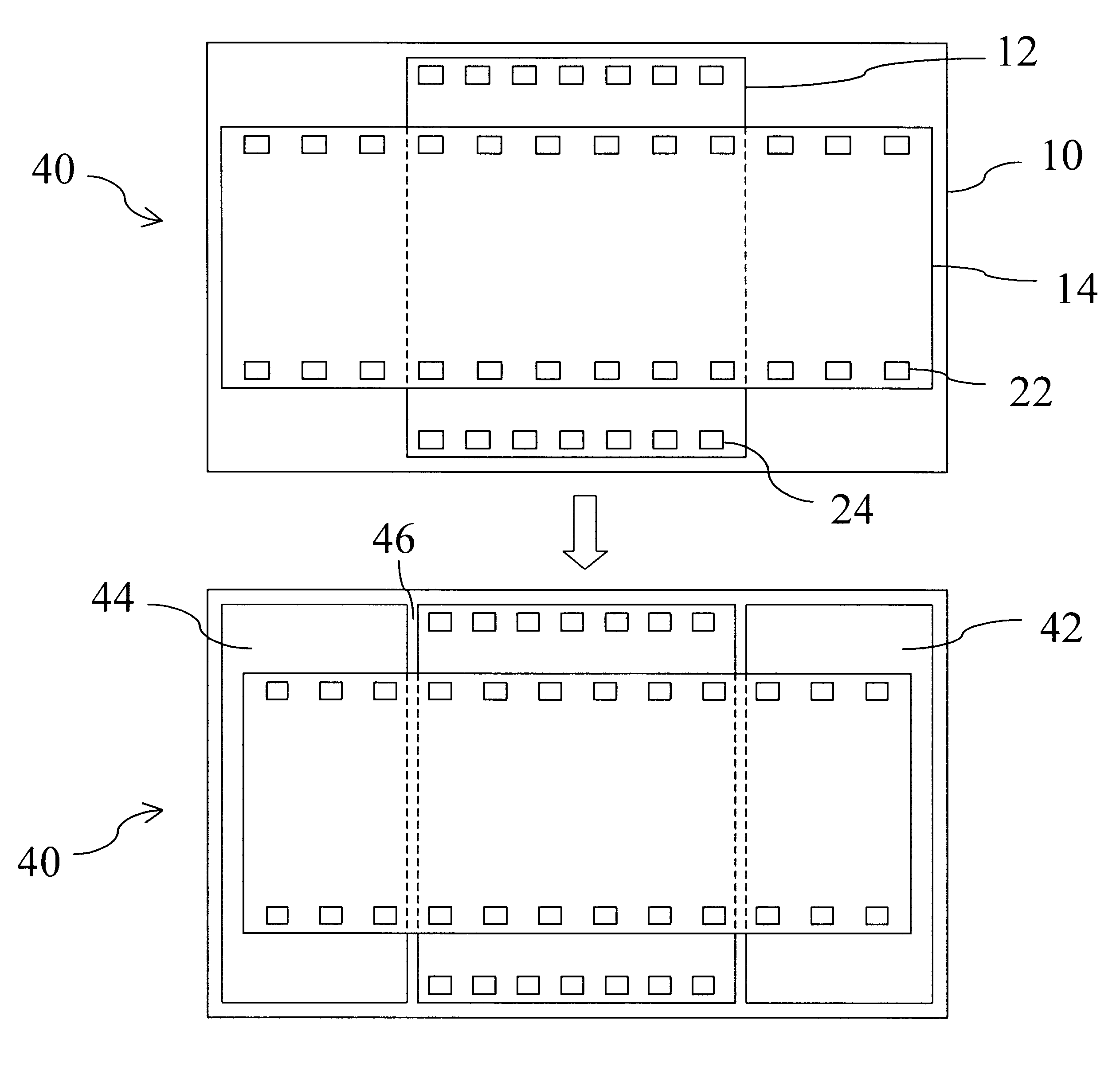
As shown in FIG. 4, in a stacked CSP structure 40, a lower chip 12 and an upper chip 14 are stacked on a substrate 10. Each interface is bonded with adhesive. The adhesive can be silver epoxy. A plurality of bonding pads 22 and 24 are disposed on the upper chip 14 and the lower chip 12, respectively. The size of the upper chip 14 is larger than that of the lower chip 12 along the direction without the bonding pads 22. Therefore, two side regions of the upper chip 14 are suspended relative to the lower chip 12. The bonding pads 22 and 24 are properly arranged two opposite sides of the upper chip 14 and the lower chip 12 so that the two rows of bonding pads 22 of the upper chip 14 are parallel to the two rows of bonding pads 24 of the lower chip 12.
In order to ov...
PUM
 Abstract
Description
Claims
Application Information