Active-matrix in-plane switching mode LCD panel having multiple common electrode voltage sources

a technology of in-plane switching mode and active matrix, which is applied in the direction of identification means, instruments, optics, etc., can solve the problems of narrow viewing angle, stains in pixels, and the mode of the lcd panel is not suited to a variety of applications

Inactive Publication Date: 2003-11-11
VISTA PEAK VENTURES LLC
View PDF7 Cites 29 Cited by
  • Summary
  • Abstract
  • Description
  • Claims
  • Application Information

AI Technical Summary

Problems solved by technology

This mode of the LCD panel, however, has the drawback of a narrow viewing angle wherein the refractive index of the LC layer largely depends on the viewing angle for the LCD panel, because the directors of the LC molecules are oriented in the direction normal to the substrate surface during application of the drive voltage.
Thus, this mode of the LCD panel is not suited for a variety of applications which require a wider viewing angle.
The DC voltage component generating the flicker in the other two of the color layers also causes the burning, irregularity and stains in the pixels to degrade the reliability of the LCD panel.
The time constant my be reduced to some extent by a larger width of the scanning signal line, which however decreases the ratio of the area for the opening to the entire pixel area and thus decreases the brightness of the screen or increases the power dissipation of the LCD panel, thereby degrading the performance of the LCD panel.
However, a lower accuracy of the relative locations between the TFT panel and the counter panel necessitates a larger shield area between the pixels, and reduces the light transmittance.
It is to be noted that a fine patterning for the transparent electrode is difficult to achieve due to the material itself.
The increase in the number of electric leads between the TFT panel and the counter panel complicates the fabrication process.
However, there is no teaching that teaches the application of respective voltages to the common electrode lines for the purpose of correction of the irregularity in the feed-through voltage of the pixels having different color layers, the irregularity being caused by the pulse delay of the scanning signal.

Method used


Image

  • Active-matrix in-plane switching mode LCD panel having multiple common electrode voltage sources
  • Active-matrix in-plane switching mode LCD panel having multiple common electrode voltage sources
  • Active-matrix in-plane switching mode LCD panel having multiple common electrode voltage sources

Examples


first embodiment

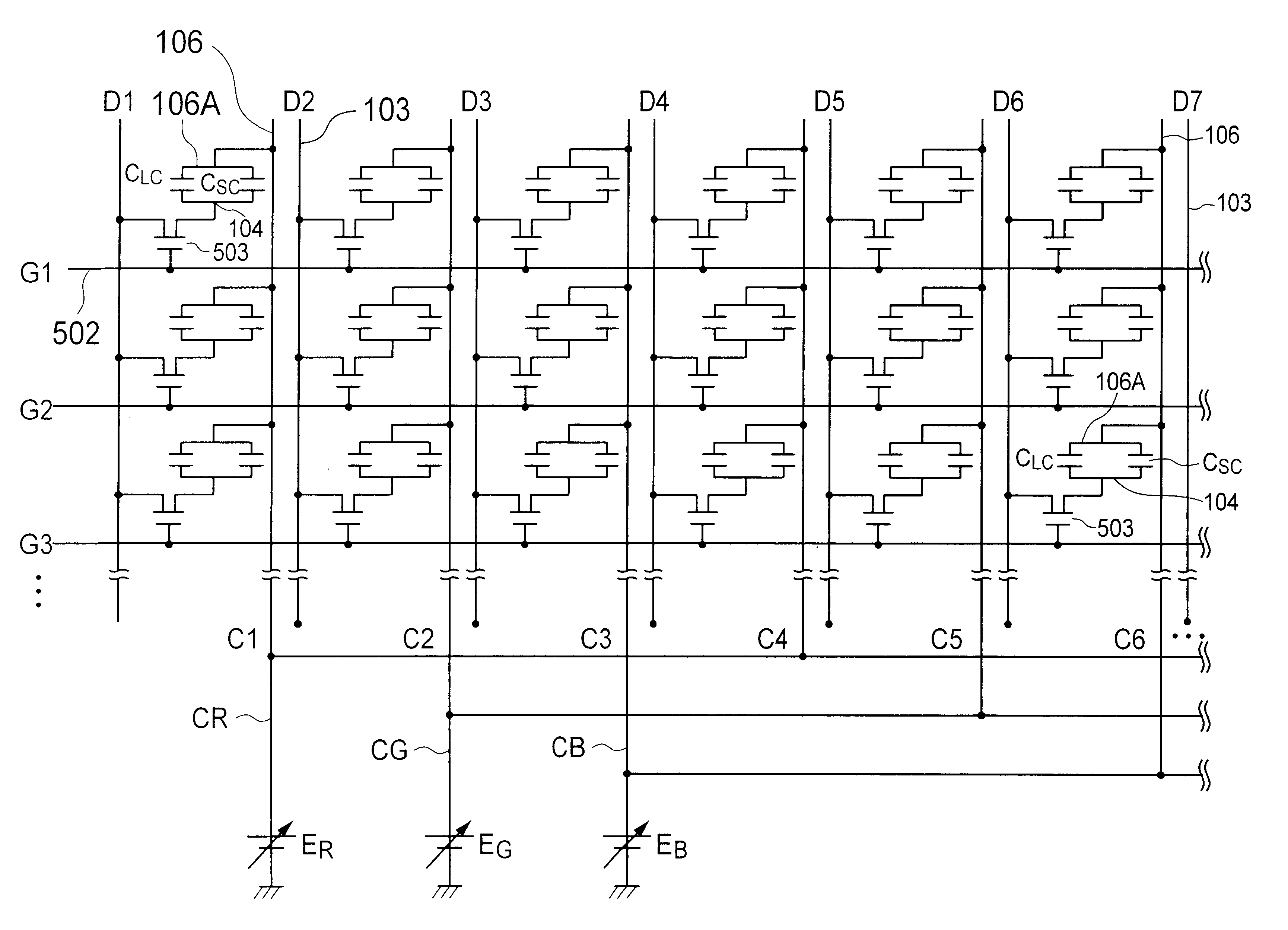
A LCD panel according to the present embodiment has an array of pixels having respective color layers, and the arrangement of color layers for respective pixels are shown in FIG. 10, as an example. Specifically, three "R", "G" and "B" colors appear consecutively or alternately in the row direction of the array of pixels, with one of the three colors iteratively appearing along the column direction.

Referring to FIG. 11 showing the equivalent circuit for the LCD panel of the present embodiment similarly to FIG. 4, each of the common electrode lines C1, C2, C3 . . . extends in the column direction and connected to pixels arranged in each column for specifying one of three colors. Each of three common electrode lines C1, C2 and C3, or C4, C5 and C6, or . . . is connected to a fourth common electrode line as counted from the each of the three common electrode lines. Thus, all the pixels defining one of the three colors are connected to a corresponding common electrode bus line CR, CG or ...

third embodiment

Referring to FIG. 15, a LCD panel according to the present invention has column spacers 504 formed by patterning. The patterned column spacer 504 has a rectangular cross section. The configuration of the patterned column spacer is described in JP-A-5-224235, for example. It is to be noted that these column spacers are not necessarily formed in respective pixel areas in the LCD panel, which causes a difference in the total capacitance between the pixels however. In the present embodiment, the difference in the total capacitance can be compensated by applying respective voltages to the common electrode lines depending on the total capacitances between the pixel electrode and the common electrode line. That is, pixels, type "A", each having therein a patterned column spacer 504 are connected to a first group of common electrode lines 106 whereas pixels, type "B", each having therein no patterned spacer are connected to another group of common electrode lines 106.

More specifically, with...

fourth embodiment

Referring to FIG. 17, a LCD panel according to the present invention reduces the flicker, burning, irregularity and stains caused by the difference in the feed-through voltage between the left side and the right side of the screen due to the delay in the scanning signal "G", as encountered in the conventional panel. In FIG. 17, common electrode lines C1 to C.sub.k, and C.sub.k+1 to Cn extend in the column direction, and connected to adjacent common electrode lines via respective resistors r.sub.1 to r.sub.k-1 and r.sub.k to r.sub.n. Some common electrode lines, for example, three common electrode lines C1, Ck and Cn are applied with respective variable voltages E1, E2 and E3, which are independently adjusted by variable voltage sources disposed in the LCD driver.

The variable voltage sources E1, E2 and E3 are adjusted depending on the field-through voltages to control the potential of the common voltage lines 106. More specifically, the potentials of the common voltage lines 106 are ...


PUM

PropertyMeasurementUnit
dielectric constantaaaaaaaaaa

Abstract

An in-line switching mode LCD panel has three groups of common electrode lines corresponding to three colors defined by color layers in the pixels. The potentials of the groups of the common electrode lines are adjusted independently of one another so that the flicker level for the corresponding pixels assumes a minimum by compensating the difference in the feed-through voltage between the pixels.

Description

(a) Field of the InventionThe present invention relates to an active-matrix in-plane switching mode LCD panel, and more particularly, to an improvement of an active-matrix LCD (liquid crystal display) panel driven by an in-plane electric field.(b) Description of the Related ArtLCD panels are generally categorized by the mode of the liquid crystal into a plurality of types including one driven by a perpendicular electric field, such as a TN-mode (twisted nematic mode) LCD panel. In this mode of the LCD panel, the orientations of the directors (axes) of the LC molecules are changed by application of a perpendicular electric field which is normal to the substrate surface, to thereby control the transparency thereof (or transmittance of light passing therethrough) for image display on the display panel. This mode of the LCD panel, however, has the drawback of a narrow viewing angle wherein the refractive index of the LC layer largely depends on the viewing angle for the LCD panel, becau...

Claims


Application Information

Patent Timeline
Patent Type & Authority Patents(United States)
IPC IPC(8): G02F1/1335G02F1/13G02F1/1343G09G3/36G09F9/30G02F1/133G02F1/1368
CPCG02F1/133514G02F1/134363G09G3/3648G09G3/3655G09G3/3607G09G2320/0247G09G2300/0434G09G2320/0204G09G2320/0219G09G2320/0223G02F1/1343
Inventor WATANABE, MAKOTOWATANABE, TAKAHIKO
Owner VISTA PEAK VENTURES LLC
Why Eureka
Try Eureka