

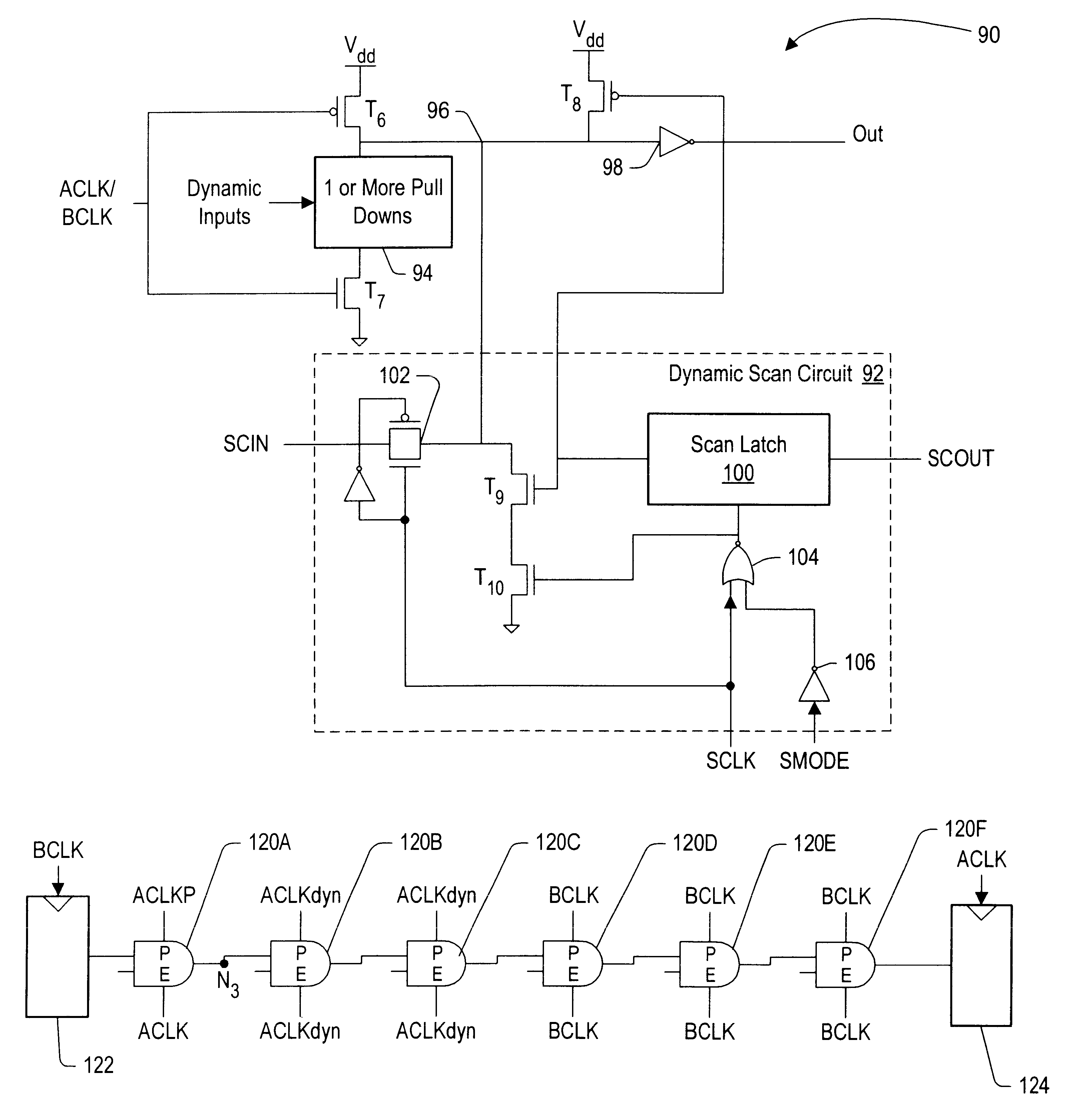
Dynamic scan circuitry for B-phase
a dynamic scan and circuit technology, applied in pulse generators, instruments, pulse techniques, etc., can solve the problems of limiting the ability to use scan to test dynamic circuits, increasing the complexity of integrated circuits, and not being fully tested for dynamic circuits
- Summary
- Abstract
- Description
- Claims
- Application Information
AI Technical Summary
Benefits of technology
Problems solved by technology
Method used
Image

Examples
Embodiment Construction
Conditional Clocking
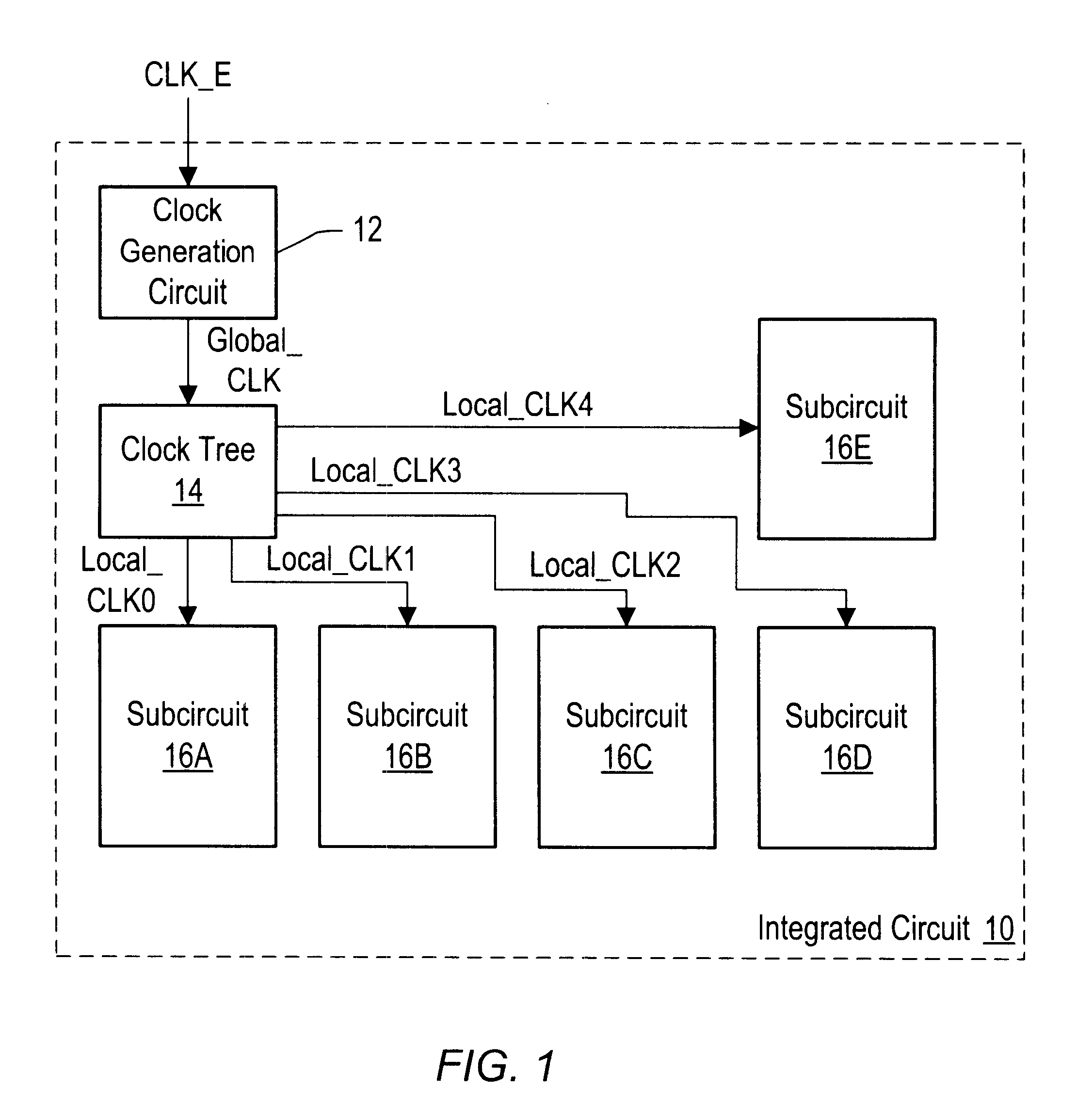
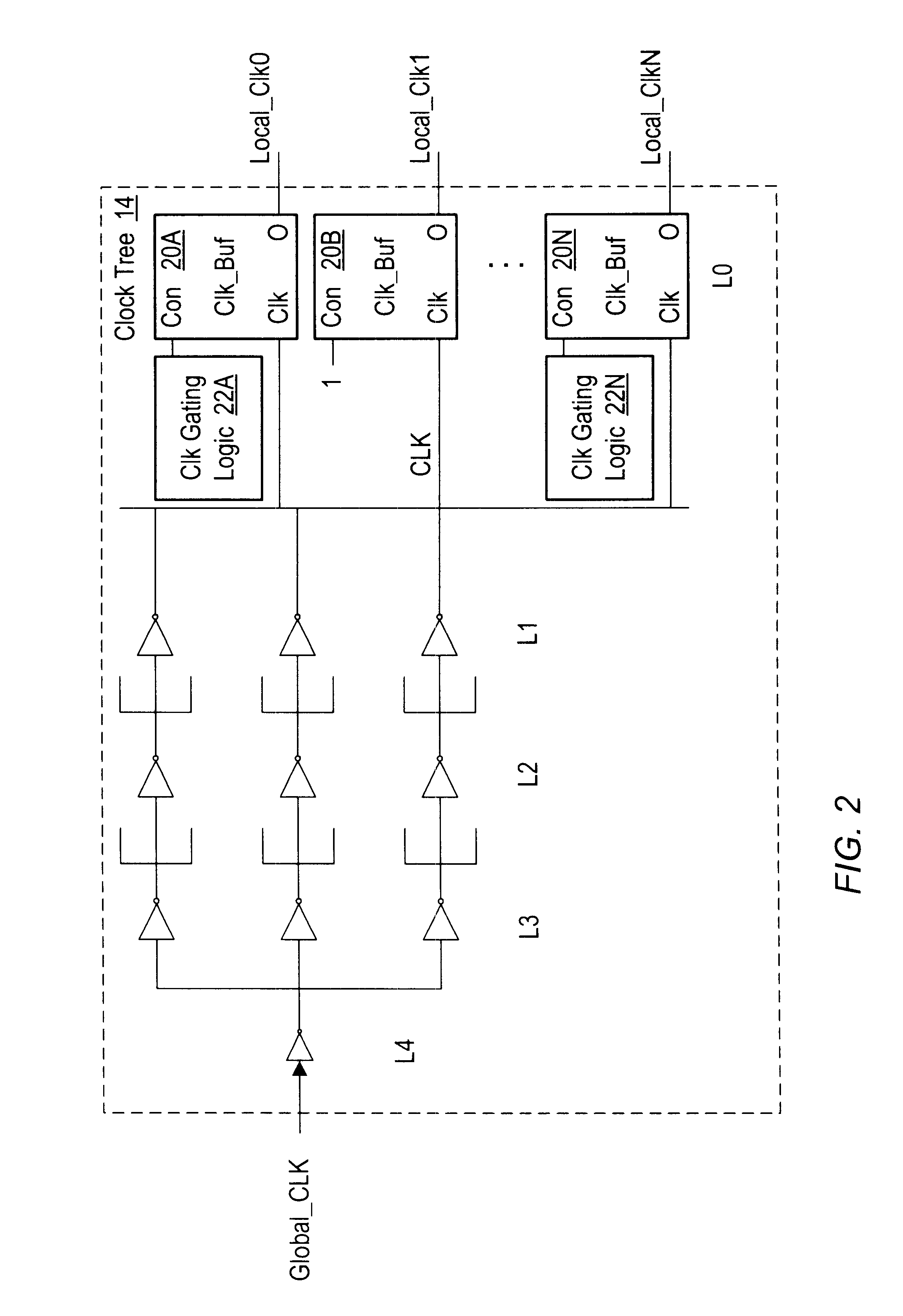
Turning now to FIG. 1, a block diagram of one embodiment of an integrated circuit 10 is shown. Other embodiments are possible and contemplated. In the embodiment of FIG. 1, the integrated circuit 10 includes a clock generation circuit 12, a clock tree 14, and a plurality of subcircuits 16A-16E. The clock generation circuit 12 is coupled to receive an external clock (CLK_E) and generate a global clock (Global_CLK) therefrom. The clock tree 14 is coupled to receive the global clock and to provide various local clocks (e.g. Local_CLK0, Local_CLK1, Local_CLK2, Local_CLK3, and Local_CLK4 to subcircuits 16A-16E, respectively).
The clock generation circuit 12 is configured to generate the global clock Global_CLK from the external clock CLK_E for use by the circuitry illustrated in FIG. 1. The clock generation circuit 12 may include, for example, a phase locked loop (PLL) for locking the phase of the global clock to the external clock. The PLL or other clock generation ci...
PUM
 Abstract
Description
Claims
Application Information