Photonic component package and method of packaging

a technology of applied in the field of photonic component package and packaging method, can solve the problems of not enabling the low cost application of conventional and low cost package manufacturing method and suitable materials known in the art, such as ceramic or plastic, and not considering or providing optional orientations for insertion of the package into a larger system. , to achieve the effect of reducing the requirement of footprint and increasing mechanical stability

Inactive Publication Date: 2004-04-06
GUANGZHOU YINXUN OPTIVIVA
View PDF19 Cites 4 Cited by
  • Summary
  • Abstract
  • Description
  • Claims
  • Application Information

AI Technical Summary

Benefits of technology

It is an object of certain preferred embodiments of the present invention to provide a photonic component package having a reduced footprint requirement for mounting onto a module and coupling to one or more optical fibers, wherein a length of at least one the optical fiber proximate to the photonics component package is substantially parallel to a mounting surface of the module.
It is an object of certain other alternate preferred embodiments of the present invention to provide a boot that at least partially encloses a photonic element coupled with a photonic component package, and wherein the boot and the photonic component package have increased mechanical stability when the photonic component package is attached to a module.
It is an object of the present invention to provide a package for a photonic component that (1) presents a reduced footprint requirement, (2) that enables an optical coupling of a photonic element and a semiconductor die, and (3) supports electrical communications between the semiconductor die module, the module comprising a printed circuit board, an electronic circuit, subsystem or system. A footprint of the package is defined as the cross-sectional area of the module, or of a mounting surface of the module, that is required to be available for use in mounting the present invention to the module.
A third preferred embodiment of the present invention further comprises a boot, wherein the boot protects and at least partially encloses an external photonic element and a photonic inlet, and enables the photonic coupling of the external photonic element and the semiconductor die. The boot includes a boot opening, a boot hole, a planar base and an upper wall. The upper wall and the planar base at least partially enclose the photonic inlet. The upper wall may be or comprise a curved surface, or a partially cylindrical surface, or one or more flat surfaces. The boot opening enables the at least partial insertion of the external element into the boot. The base provides a planar surface, wherein the planar surface is placed in mechanical contact with a module when the third preferred embodiment of the present invention is electrically coupled with the module. The boot thereby provides increased mechanical stability of the package when the package is mounted onto the module.
The substantially flat and planar surfaces of the base, the top surface, and the two side surfaces provide surface areas that are easier and less expensive to mark and add signage to than curved or non-flat surfaces. Automated mounting and handling systems more efficiently grasp and position the boot due to the flatness of the base, the top surface, and the two side surfaces, in contrast to prior art housings or boots that are curved or non-planar. The flatness and orientation of the base, top surface, and both side surfaces enable more efficient packing and shipping of the boot of the third preferred embodiment over the prior art.

Problems solved by technology

But the disclosure of Kato et al. fails to consider or provide optional orientations for insertion of the package into a larger system.
Kato et al. does not address the advantages of installing the package onto a printed circuit board after high temperature manufacturing steps of the printed circuit board are completed.
Iida et al. does not enable the low cost application of conventional and low cost package manufacturing methods and suitable materials known in the art, such as ceramic or plastic.
Yet La's work is limited to the provision of a device that accepts and emits electrical and photonic signals via a plurality of electricity-to-light and light-to-electricity converters and wherein all of the converters are aligned along the same side of a substrate.
La fails to provide or consider a generally applicable package or packaging technique that enables a coupling of a photonic element, e.g., an optical fiber, or a collimator, with a MEMS or semiconductor device and within or via a low cost and standard package size and type.

Method used


Image

  • Photonic component package and method of packaging
  • Photonic component package and method of packaging
  • Photonic component package and method of packaging

Examples


Embodiment Construction

While the description above provides a full and complete disclosure of the preferred embodiments of the present invention, various modifications, alternate constructions, and equivalents will be obvious to those with skill in the art. Thus the scope of the present invention is limited solely by the appended claims.

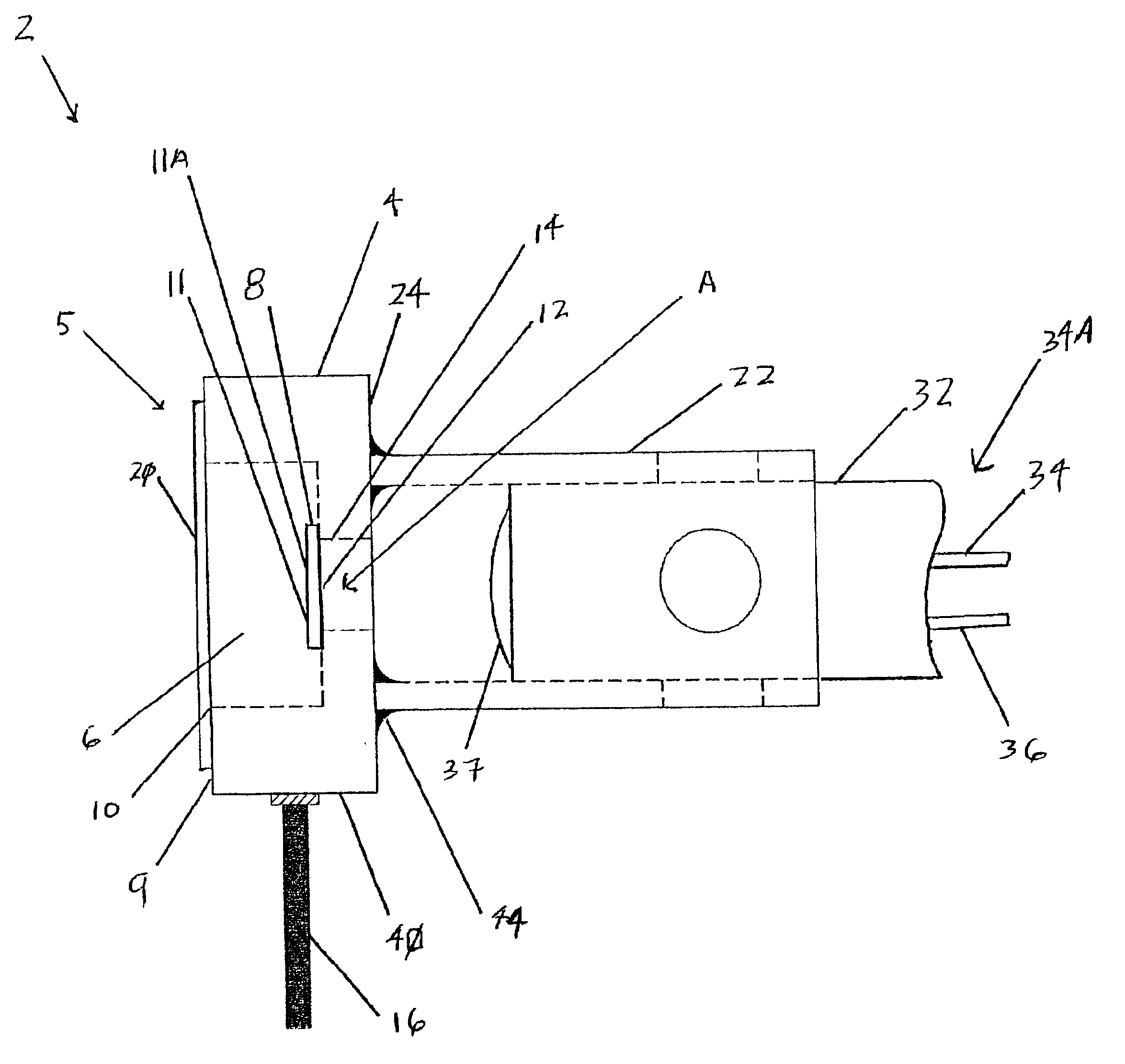
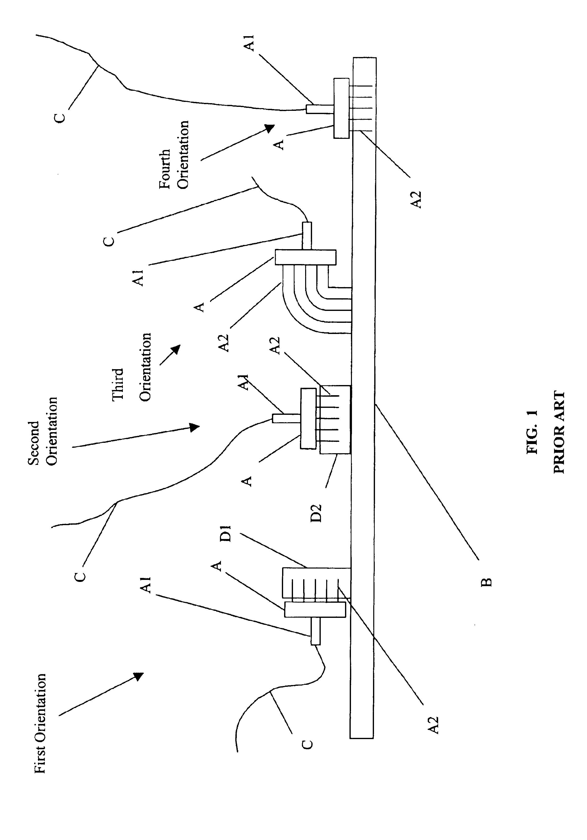
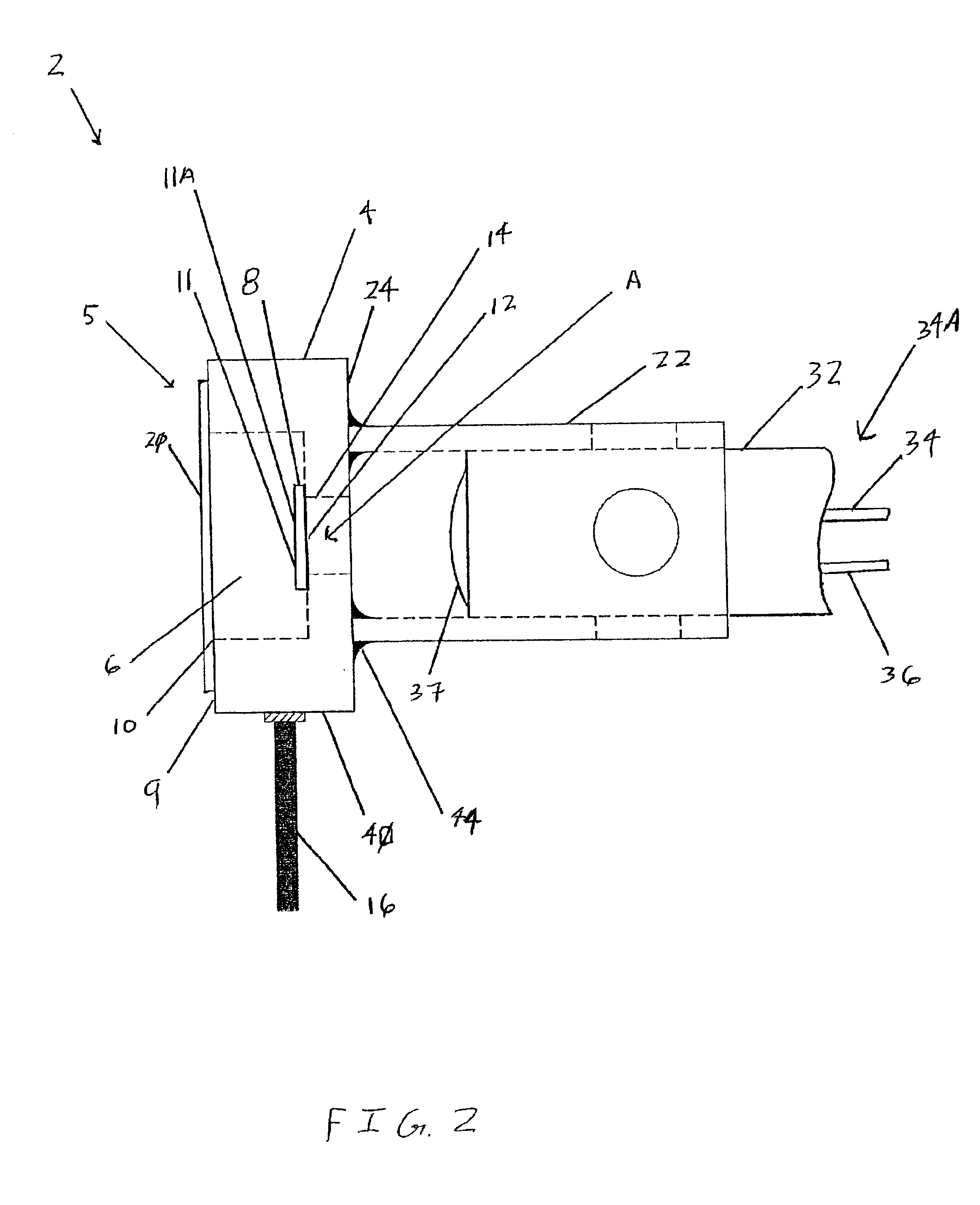
Referring now generally to the Figures and particularly to FIG. 1, FIG. 1 is a cross-sectional view of four orientations of a prior art photonic component A coupled with a PC board B. A collimator A1 of the prior art device A is coupled with an optical fiber C. In a first orientation a plurality of pins A2 are inserted into a socket D1, whereby the pins A2 are place in parallel with the PC Board B. In a second orientation the plurality of pins A2 are inserted downwards and towards the PC Board and into a socket D2. In a third configuration the plurality of pins A2 are extended in length and bent downwards towards a direct mechanical coupling with the PC board B. In a fourt...


PUM


Abstract

A method of packaging a photonic component and a photonic component package are provided. The package comprises a package body a set of pins, wherein the orientation of the pins does not increase the footprint requirements of the package when the package is mounted onto a module. A semiconductor die is attached to and enclosed within the package. The die may be a MEMS and may include a movable mirror. An optical fiber is attached in a parallel orientation to a mounting surface of the module. The package is a low cost part with pins attached on a pinout side. An optional photonic inlet of the package is additionally coupled with one or more external photonic elements. The photonic inlet is positioned relative to a through hole to allow light to travel between the MEMS die and the external photonic element. The photonic inlet and one or more external photonic elements may be partially enclosed by a boot that provides increased mechanical stability when the package is coupled with a printed circuit board.

Description

The present invention relates to photonic component packages, and more particularly to methods of fabricating photonic component packages with reduced footprint requirements.Photonic components are of increased benefit when reduced in size and cost. The cross-sectional area of a surface of an electronic module, subsystem, or system that is taken up by, or devoted to, a certain photonic component is referred to as the footprint of that component. The footprint required to couple or interface a photonic component with a printed circuit board or an electronic circuit, module, system, subsystem or socket is typically related to the design of the package of the component that encloses the photonic and electronic elements of the device. In particular, the need to couple or attach photonic elements, such as optical fibers, to photonic components creates needs in the art for improvement in the design of photonic component packages.Kato, et al., in "Optical module, method for manufacturing o...

Claims


Application Information

Patent Timeline
Patent Type & Authority Patents(United States)
IPC IPC(8): G02B6/35G02B6/42
CPCG02B6/3582G02B6/4201G02B6/3512G02B6/3598
Inventor VAGANOV, VLADIMIN
Owner GUANGZHOU YINXUN OPTIVIVA
Why Eureka
Try Eureka