Nonvolatile memory cells having split gate structure and methods of fabricating the same

a technology of nonvolatile memory cells and gate structures, which is applied in the field of semiconductor devices, can solve problems such as devices losing their stored data

Inactive Publication Date: 2004-06-22
SAMSUNG ELECTRONICS CO LTD
View PDF3 Cites 33 Cited by
  • Summary
  • Abstract
  • Description
  • Claims
  • Application Information

AI Technical Summary

Problems solved by technology

Volatile memory devices lose their stored data when their power supply is interrupted, and nonvolatile memory devices retain their stored data even when their power supply is interrupted.

Method used


Image

  • Nonvolatile memory cells having split gate structure and methods of fabricating the same
  • Nonvolatile memory cells having split gate structure and methods of fabricating the same
  • Nonvolatile memory cells having split gate structure and methods of fabricating the same

Examples


Embodiment Construction

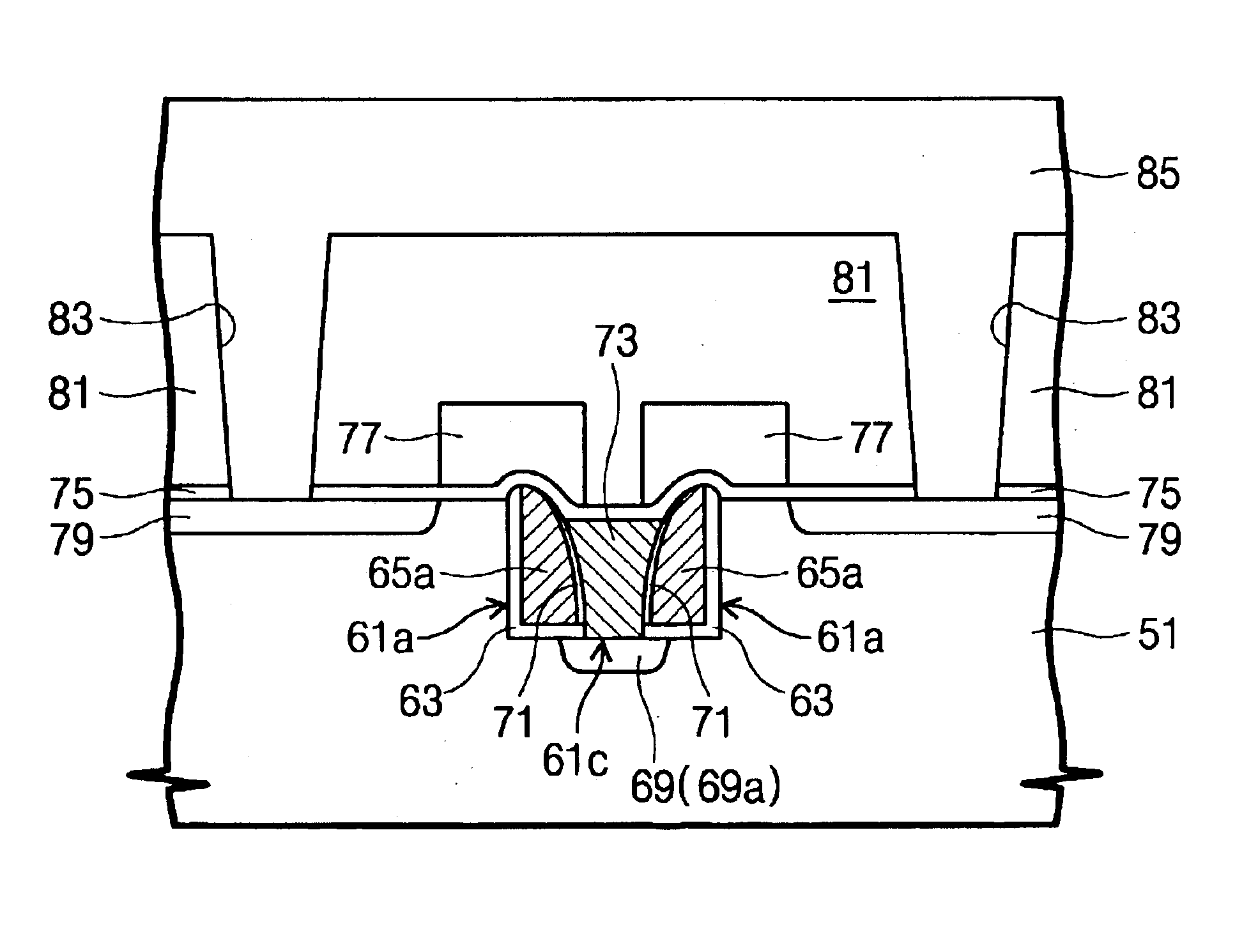
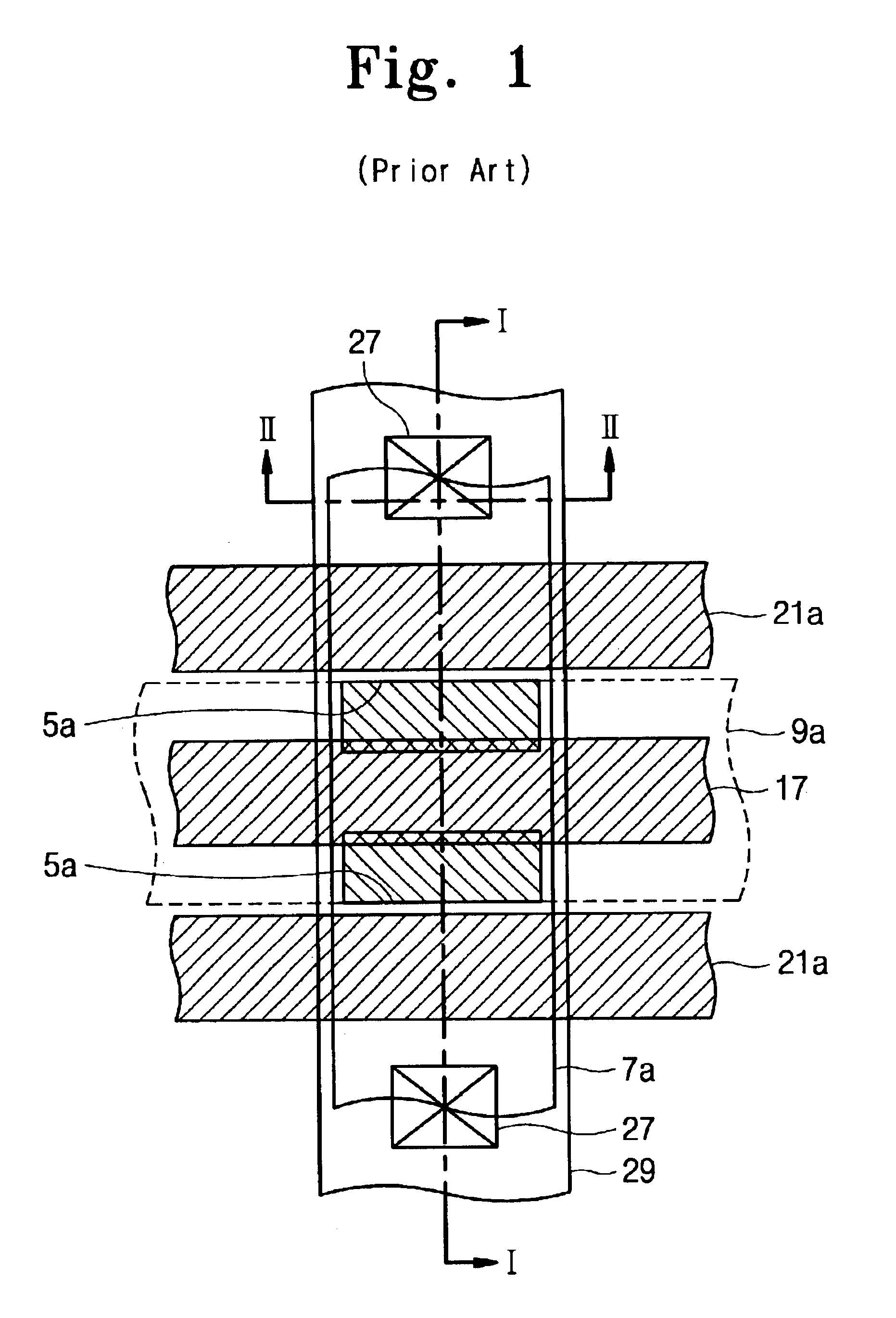
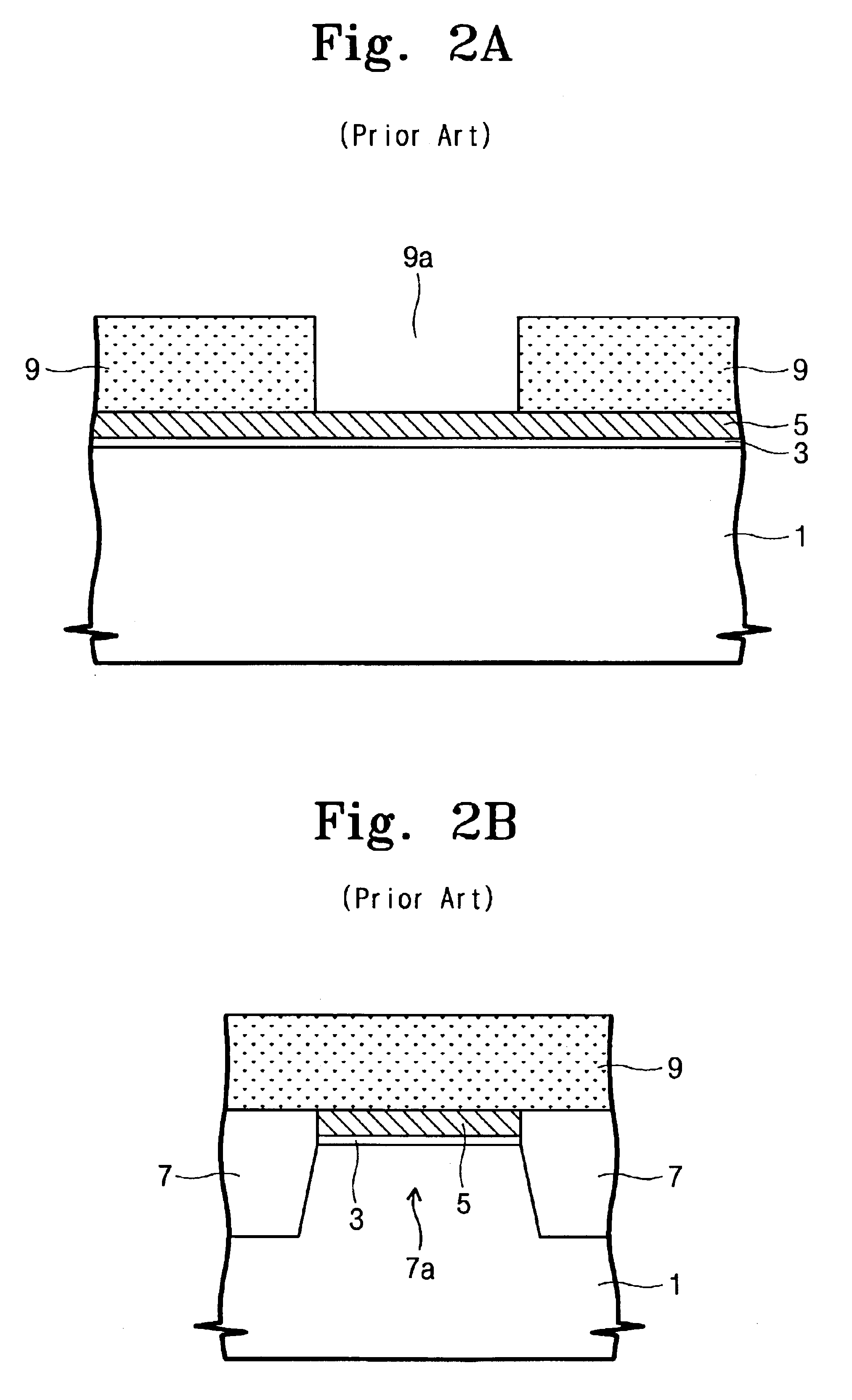
The present invention will now be described more fully hereinafter with reference to the accompanying drawings, in which preferred embodiments of the invention are shown. The invention may, however, be embodied in different forms and should not be construed as limited to the embodiments set forth herein. Rather, these embodiments are provided so that this disclosure will be thorough and complete, and will fully convey the scope of the invention to those skilled in the art. In the drawings, the thickness of layers and regions are exaggerated for clarity. It will also be understood that when a layer is referred to as being "on" another layer or substrate, it can be directly on the other layer or substrate, or intervening layers may also be present. Like numbers refer to like elements throughout.

FIG. 7 is a top plan view of nonvolatile memory cells in accordance with a preferred embodiment of the present invention. FIGS. 8A, 9A, 10A, 11A, 12A, 13A, and 14A are cross-sectional views tak...


PUM


Abstract

Nonvolatile memory cells having a split gate structure and methods of fabricating the same are provided. The nonvolatile memory cells include active regions defined at a predetermined region of a semiconductor substrate. A portion of each of the active regions is etched to form a cell trench region. Insulated floating gates are disposed on a pair of sidewalls parallel with the direction that crosses the active region. A source region is disposed at a bottom surface of the cell trench region. A gap region between the floating gates is filled with a common source line electrically connected to the source region. The common source line is extended along the direction that crosses the active regions. The active regions, which are adjacent to the floating gates, are covered with word lines parallel with the common source line. Drain regions are disposed in the active regions adjacent to the word lines. The drain regions are electrically connected to bit lines that cross over the word lines.

Description

This application claims priority to Korean Patent Application No. 2002-17090, filed on Mar. 28, 2002, the contents of which are herein incorporated by reference in their entirety.1. Field of the InventionThe present invention relates, generally, to semiconductor devices and methods of fabricating the same. More specifically, the present invention is directed to nonvolatile memory cells having a split gate structure and methods of fabricating nonvolatile memory cells having a split gate structure.2. Discussion of Related ArtSemiconductor memory devices for storing data can be typically categorized as either volatile memory devices or nonvolatile memory devices. Volatile memory devices lose their stored data when their power supply is interrupted, and nonvolatile memory devices retain their stored data even when their power supply is interrupted. Accordingly, the nonvolatile memory devices have been widely used in memory cards, mobile telecommunication systems or the like.The nonvolat...

Claims


Application Information

Patent Timeline
Patent Type & Authority Patents(United States)
IPC IPC(8): H01L27/115H01L21/70H01L21/8247G11C16/06H01L29/788H01L29/792
CPCH01L27/115H01L27/11556H10B41/27H10B69/00G11C16/06
Inventor KIMKIM, DONG-JUNCHO, MIN-SOOKIM, DAI-GEUN
Owner SAMSUNG ELECTRONICS CO LTD
Why Eureka
Try Eureka