Thickness measuring apparatus, thickness measuring method, and wet etching apparatus and wet etching method utilizing them

a technology of thickness measurement and thickness measurement, which is applied in the direction of measurement devices, semiconductor/solid-state device testing/measurement, instruments, etc., can solve the problems of inability to measure the thickness of the semiconductor wafer at a high speed, and achieve the effect of efficiently reducing the influence of error variation and the lik

a technology of thickness measurement and thickness measurement, which is applied in the direction of measurement devices, semiconductor/solid-state device testing/measurement, instruments, etc., can solve the problems of inability to measure the thickness of the semiconductor wafer at a high speed, and achieve the effect of efficiently reducing the influence of error variation and the lik

US6768552B2Inactive Publication Date: 2004-07-27HAMAMATSU PHOTONICS KK

Image

  • Thickness measuring apparatus, thickness measuring method, and wet etching apparatus and wet etching method utilizing them
  • Thickness measuring apparatus, thickness measuring method, and wet etching apparatus and wet etching method utilizing them
  • Thickness measuring apparatus, thickness measuring method, and wet etching apparatus and wet etching method utilizing them

Examples


Embodiment Construction

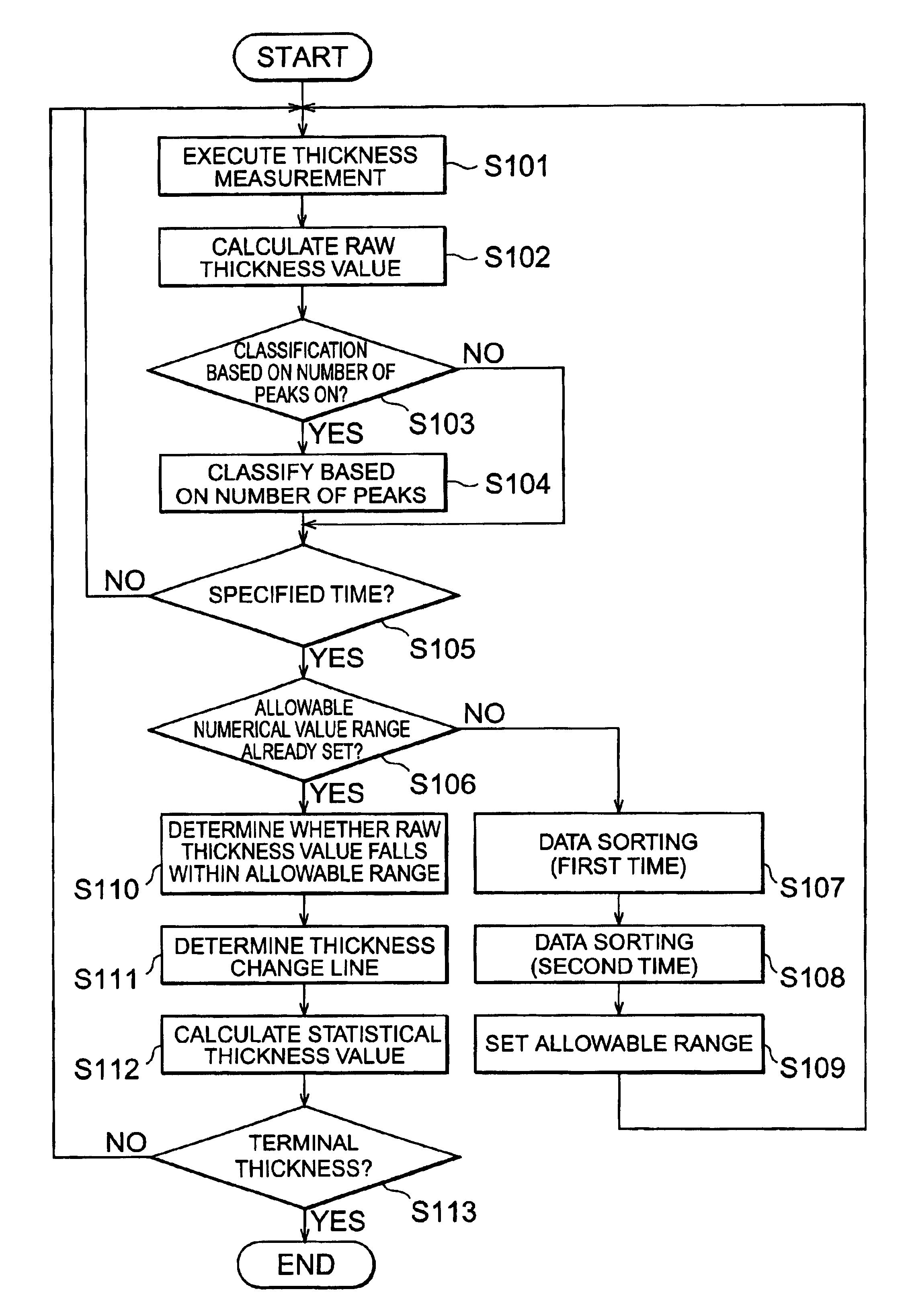
A preferred embodiment of a thickness measuring apparatus and thickness measuring method according to the present invention, and a wet etching apparatus and wet etching method using the thickness measuring apparatus and method will be described below with reference to the accompanying drawings. The same reference numerals denote the same elements throughout the description of the drawings, and a repetitive description will be omitted. The dimensional ratios in the drawings do not always match those in the description.

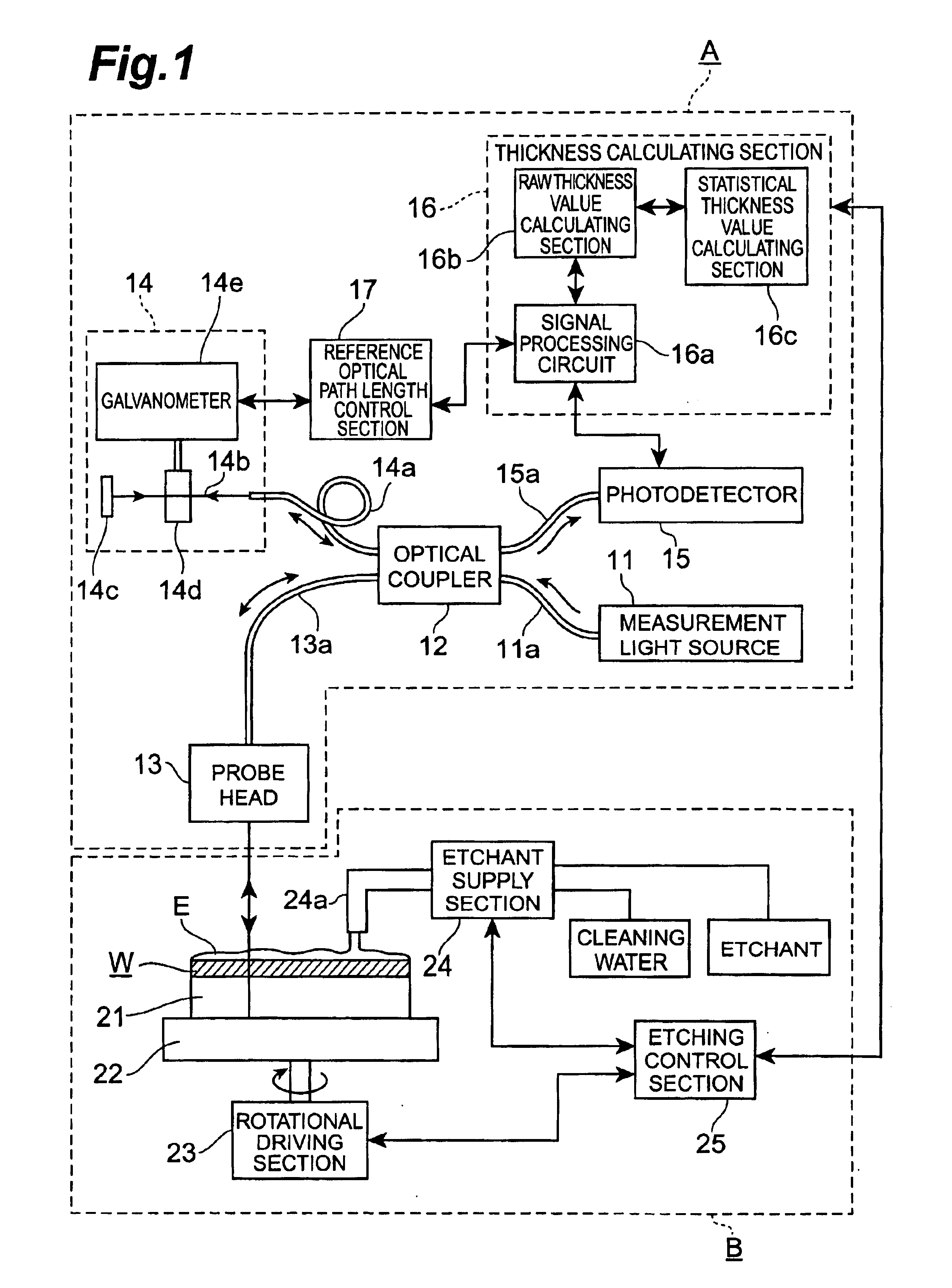
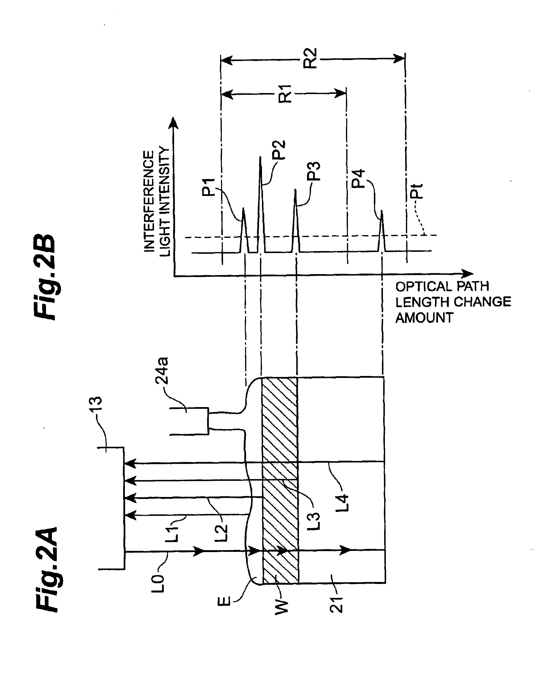
First, the arrangements of a thickness measuring apparatus and wet etching apparatus according to the present invention will be described together with steps in a corresponding thickness measuring method. FIG. 1 is a block diagram showing an embodiment of a thickness measuring apparatus and a wet etching apparatus having the thickness measuring apparatus. This wet etching apparatus comprises a thickness measuring apparatus A and a normal wet etching apparatus B except f...


PUM

PropertyMeasurementUnit
wavelengthaaaaaaaaaa
thicknessaaaaaaaaaa
optical path lengthaaaaaaaaaa

Abstract

At each measurement time, reflected light from a semiconductor wafer W or the like by measurement light from a measurement light source 11 is coupled to reference light from a reference light generating section 14, and interference light is detected by a photodetector 15. A raw thickness value calculating section 16b selects two light intensity peaks corresponding to the upper and lower surfaces of the wafer W from a light intensity distribution between an interference light intensity and a reference optical path length and calculates a raw thickness value. A statistical thickness value calculating section 16c executes statistical processing including data sorting, determination whether the raw thickness value falls within an allowable numerical value range, and determination of a thickness change line, thereby obtaining a statistical thickness value. With this arrangement, a thickness measuring apparatus and thickness measuring method capable of measuring the thickness of a semiconductor wafer during execution of wet etching independently of the presence of an etchant, and a wet etching apparatus and wet etching method using the thickness measuring apparatus and method are implemented.

Description

The present invention relates to a thickness measuring apparatus and thickness measuring method of measuring the thickness of a semiconductor wafer during execution of wet etching and a wet etching apparatus and wet etching method using the thickness measuring apparatus and method.In manufacturing semiconductor devices, recently, the necessity of an etching process for thinning a semiconductor wafer with a pattern or the like is increasing.In such an etching process, a wet etching apparatus for etching a semiconductor wafer while supplying an etchant is used. In a conventional wet etching method, a dummy wafer is etched to confirm the etching rate in advance, and the etching end time is determined on the basis of the etching rate.However, when such an etching time management method is used, an extra process for etching a dummy wafer is necessary in addition to an actual etching process. In addition, the etching rate may change for each etching process. For this reason, time manageme...

Claims


Application Information

Patent Timeline
27 Jul 2004
Publication
US6768552B2
IPC
G01B11/06; H01L21/66; H01L21/00; G01B9/02; G01B11/02; H01L21/306
CPC
G01B11/0675; G01B11/0683; H01L21/67253; H01L22/12
Inventors
TAKAHASHI, TERUO; WATANABE, MOTOYUKI