Method and apparatus for providing row redundancy in nonvolatile semiconductor memory

a non-volatile semiconductor and row redundancy technology, applied in the field of non-volatile semiconductor memory, can solve the problems of data errors in nor-type flash memory products, ineffective technique, functional failure,

Inactive Publication Date: 2004-08-03
WINBOND ELECTRONICS CORP
View PDF6 Cites 62 Cited by
  • Summary
  • Abstract
  • Description
  • Claims
  • Application Information

AI Technical Summary

Problems solved by technology

However, if the data cells in the sector start out at different threshold voltages and only a sector erase operation is performed, some of the data cells may be erased near to or into depletion which will cause data errors in NOR-type flash memory products.
However, the technique can be ine...

Method used


Image

  • Method and apparatus for providing row redundancy in nonvolatile semiconductor memory
  • Method and apparatus for providing row redundancy in nonvolatile semiconductor memory
  • Method and apparatus for providing row redundancy in nonvolatile semiconductor memory

Examples


Embodiment Construction

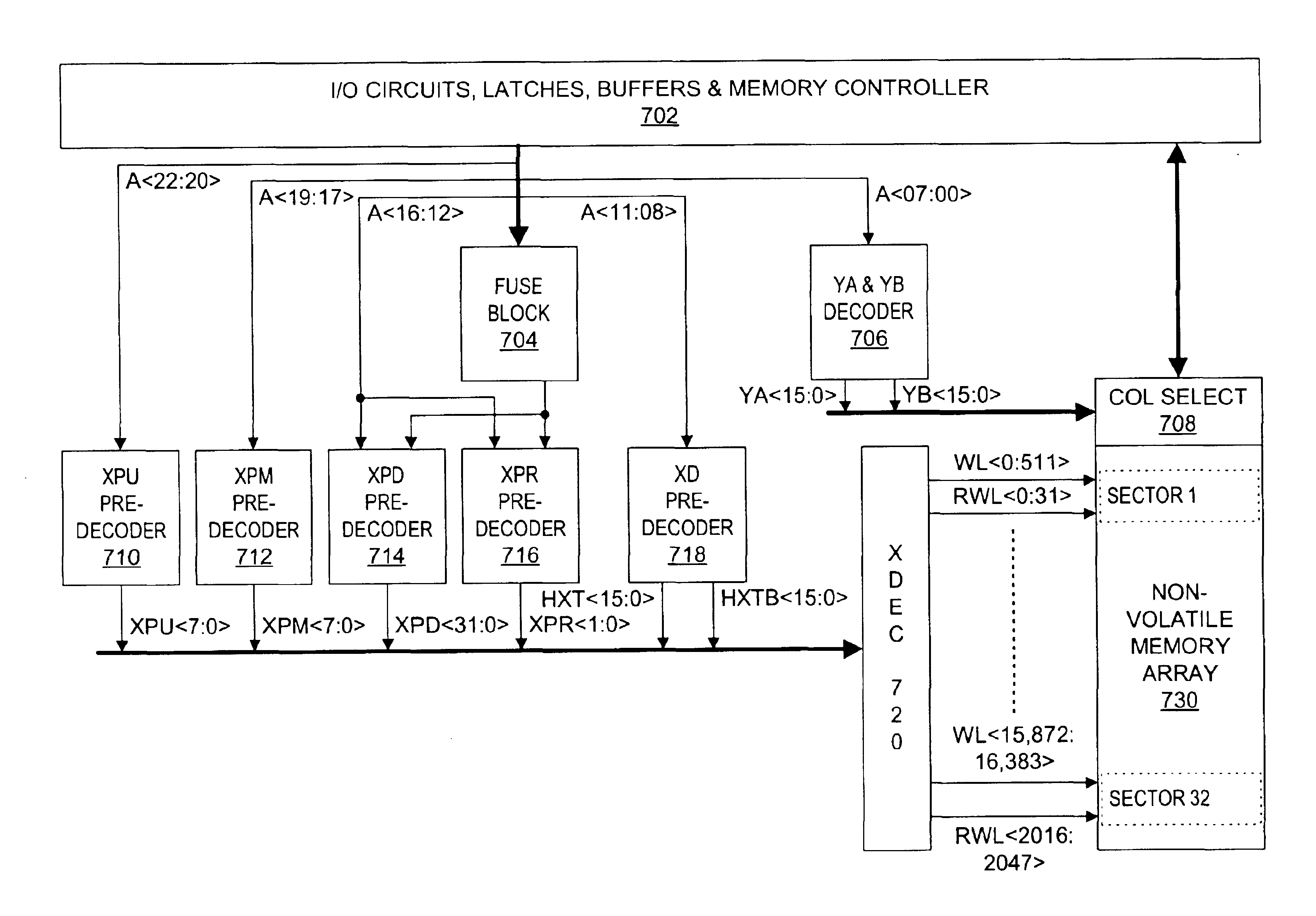
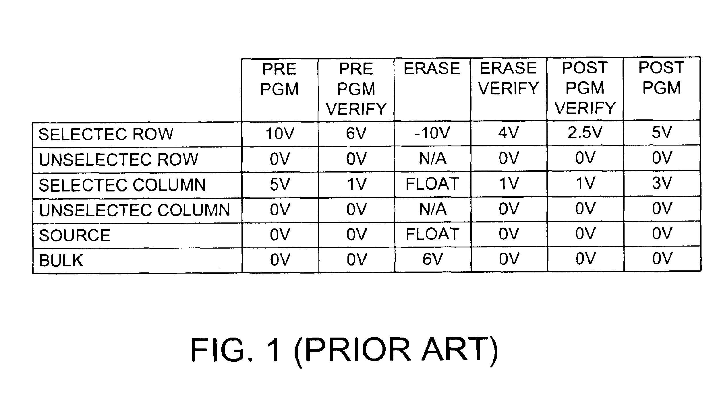
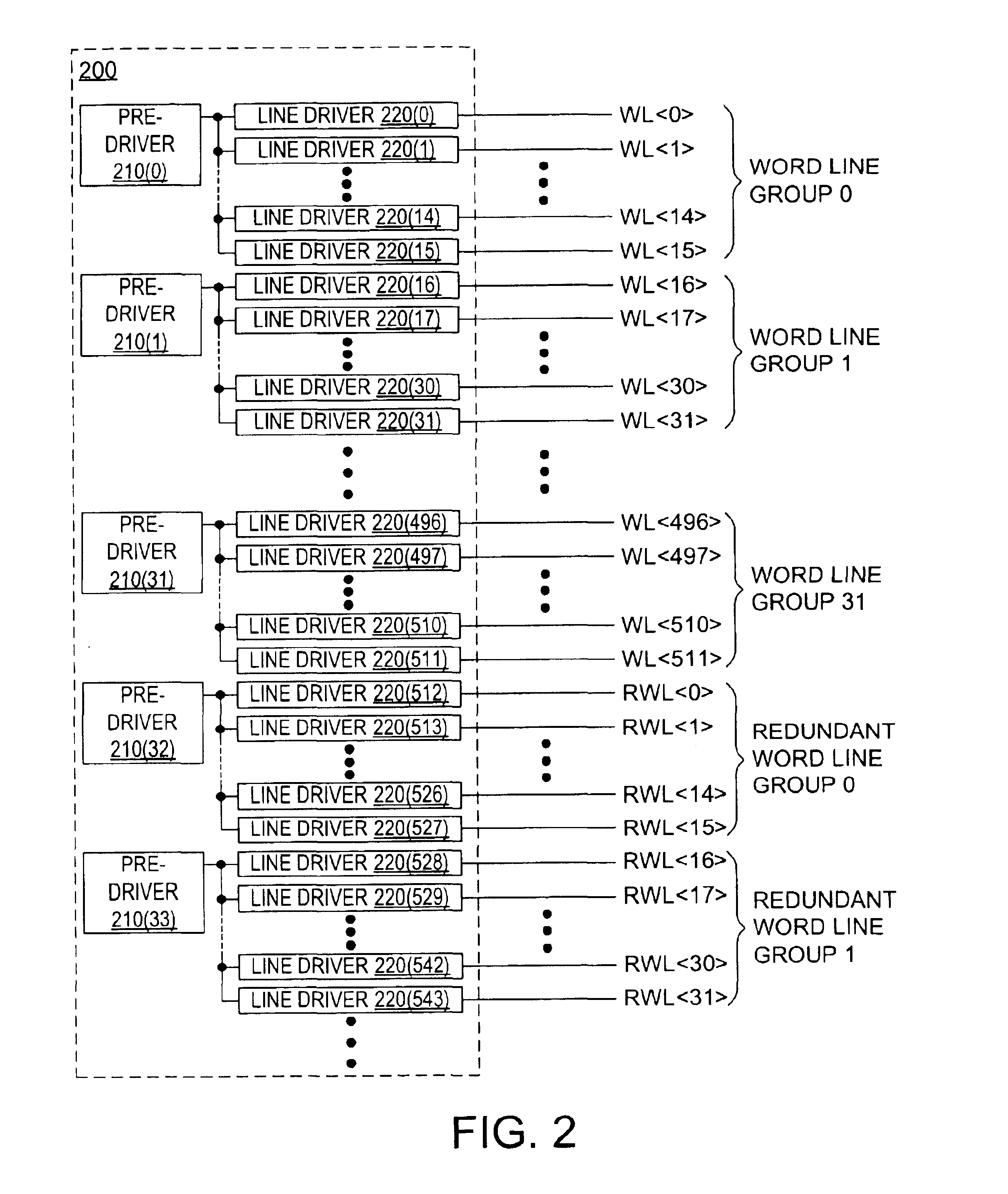
In a single transistor NOR-type flash memory of either the ETOX or virtual ground type that uses row redundancy, and illustratively wherein the erased cell threshold voltage is lower than the programmed cell threshold voltage, we have found that the typical sequence of operations used for an embedded sector erase of a selected sector, namely the Preprogram, Preprogram Verify, Erase, Erase Verify, Post-Program Verify, and Post-Program operations, need not and should not be performed for the data cells on bad or shorted rows or in unused redundant rows. Instead, the bad or shorted rows or the unused redundant rows are suitably biased so that the threshold voltages of the data cells in these rows tend to converge to a threshold voltage near the UV erased threshold. For the unselected sectors, the sector select transistors arc off so as to eliminate bit line disturb, and since each of the sectors resides in an isolated p-well, the unselected sectors do not experience bulk disturb.

An ill...


PUM


Abstract

In a NOR-type flash memory of either the ETOX or virtual ground type that is programmed using electron injection and erased using FN tunneling, and that has row redundancy, the typical sequence of operations used for an embedded sector erase, namely the Preprogram, Preprogram Verify, Erase, Erase Verify, Post-Program Verify, and Post-Program operations, need not be performed for the data cells on bad or shorted rows or in unused redundant rows. Instead, the bad or shorted rows or the unused redundant rows are suitably biased so that the threshold voltages of the data cells in these rows tend to converge to a threshold voltage near the UV erased threshold.

Description

1. Field of the InventionThe present invention relates to nonvolatile semiconductor memory, and more particularly to providing row redundancy in nonvolatile semiconductor memory.2. Description of the Related ArtNonvolatile semiconductor memory array retains stored data when power is removed. Many different types of nonvolatile data cells suitable for nonvolatile memory are known, including a class of single transistor devices that are based on the storage of charge in discrete trapping centers of a dielectric layer of the structure, and another class of devices that are based on the storage of charge on a conducting or semiconducting layer that is completely surrounded by a dielectric, typically an oxide. Techniques are also known for achieving multiple bit storage in a single transistor nonvolatile data cell by programming the multiple bits into a data cell as different voltage levels or in different parts of the cell. The trapped charge establishes the threshold voltage, or V.sub....

Claims


Application Information

Patent Timeline
IPC IPC(8): G11C16/34G11C16/08G11C16/06G11C29/00
CPCG11C16/08G11C16/3404G11C29/82
Inventor PARK, EUNGJOON
Owner WINBOND ELECTRONICS CORP
Why Eureka
Try Eureka