
Test outputs using an idle bus

a technology of output and bus, which is applied in the field of test outputs using an idle bus, can solve the problems of increasing complexity, increasing complexity, and affecting the debugging process of the circuit,

Inactive Publication Date: 2004-08-24
HEWLETT PACKARD DEV CO LP
View PDF4 Cites 23 Cited by
  • Summary
  • Abstract
  • Description
  • Claims
  • Application Information

AI Technical Summary

Benefits of technology

The present invention relates to a method for improving the testing of electronic circuits, particularly integrated circuits used in computer systems. The invention addresses the issue of limited access to internal test points on the circuit, which can make it difficult for developers to identify and fix hardware problems. The invention proposes a method for managing an idle bus to enhance the testing of integrated circuits. The method involves using a multiplexor circuit to select a subset of internal test points based on a software-configurable value. This allows developers to choose a larger number of internal test points while still limiting the number of dedicated test pins. The invention aims to provide additional test data without adding additional dedicated test pins and reduce the time and effort required to troubleshoot hardware failures.

Problems solved by technology

However, such enhanced functionality has come at the expense of complexity.
Indeed, as compared to an integrated circuit made twenty years ago, today's integrated circuits, as well as the electronic circuits in which such integrated circuits are used, are vastly more complex.
This is not the case once the circuit is actually reduced to hardware.
In testing the circuit, however, the input and output pins do not always help the person debugging the circuit, because many hardware issues within the circuit may not generate a signal on the input or output pins.
A limitation associated with the test pins is that the number of internal test points that are desirable is much larger than the output pins that are available.
Each pin on an integrated circuit increases its size, cost, and complexity.
Although such a technique allows the debugger to sample a relatively large number of internal signals using a relatively small number of test pins, the technique is not without its drawbacks.
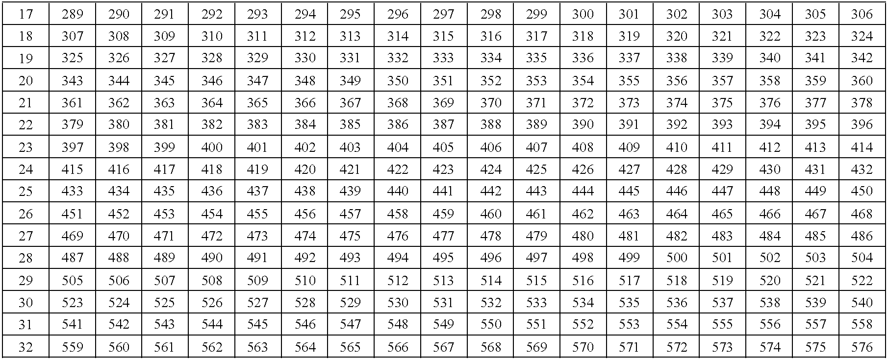
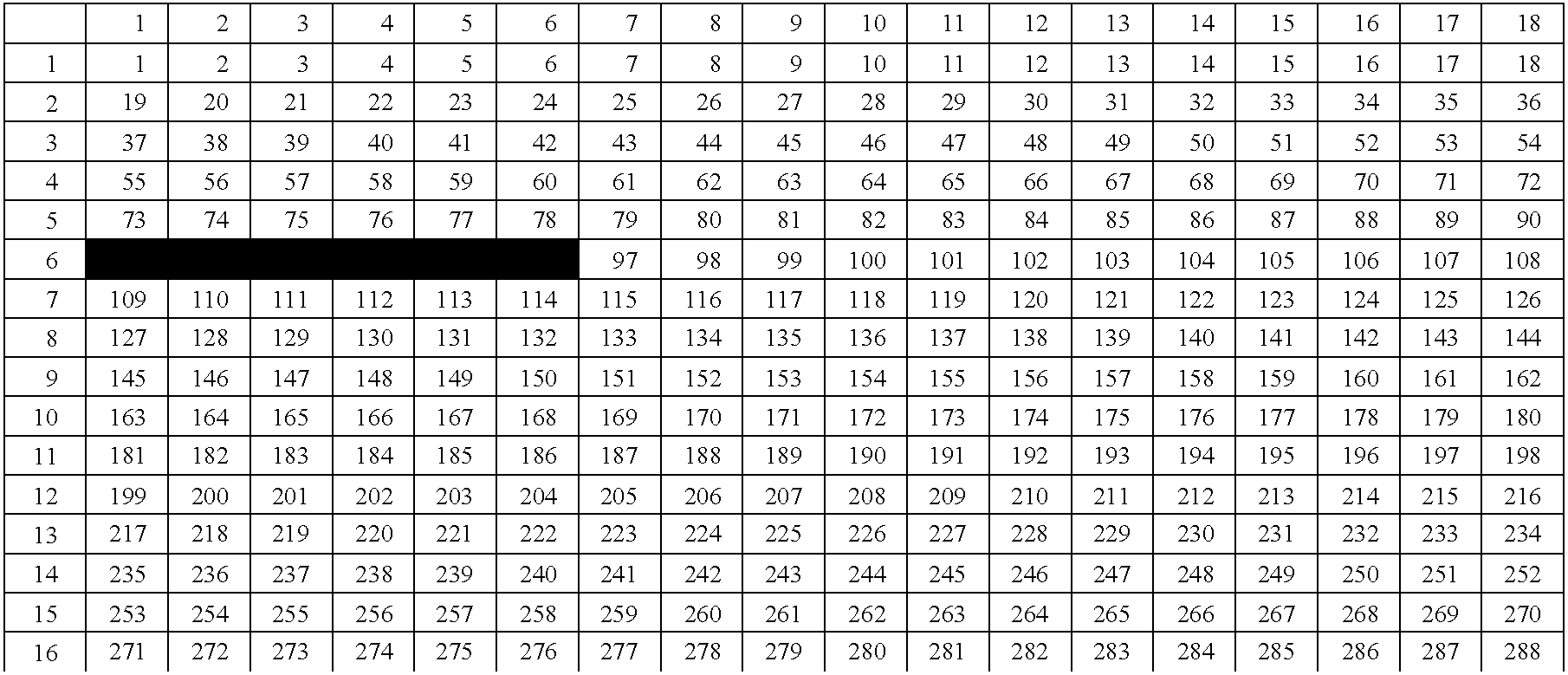
For example, a problem faced by a debugger involves the need to view simultaneously two or more signals in different sets of the 32 groups of 18 signals.
While this technique has also produced some desirable results, designers cannot accurately predict which signals will be needed in determining the root cause of a hardware problem.
As a result of these drawbacks, debuggers can often expend a significant amount of time troubleshooting a circuit to resolve failures.

Method used


Image

  • Test outputs using an idle bus
  • Test outputs using an idle bus
  • Test outputs using an idle bus

Examples


Embodiment Construction

One or more specific embodiments of the present invention will be described below. In an effort to provide a concise description of these embodiments, not all features of an actual implementation are described in the specification. It should be appreciated that in the development of any such actual implementation, as in any engineering or design project, numerous implementation-specific decisions may be made to achieve the developers' specific goals, such as compliance with system-related and business-related constraints, which may vary from one implementation to another. Moreover, it should be appreciated that such a development effort might be complex and time consuming, but would nevertheless be a routine undertaking of design, fabrication, and manufacture for those of ordinary skill having the benefit of this disclosure.

Turning now to the drawings, and referring initially to FIG. 1, a multiprocessor computer system, for example a Proliant 8500 PCI-X from Compaq Computer Corporat...


PUM


Abstract

A test circuit receives a plurality of internal test signals and delivers a group of the plurality of internal test signals onto a bus during an idle state of the bus. The bus is coupled to output pins so that the group of internal test signals can be used in debugging operations. The test circuit may include a multiplexing circuit that receives the plurality of internal test signals as inputs and that delivers a selected group of the internal test signals as outputs. The test circuit may also include a switch that couples the selected group of the internal test signals onto the bus during an idle state.

Description

The present invention relates generally to a method for enhancing the testing of an electronic circuit, such as a circuit for use in a computer system. More particularly, the present technique improves the testing of an integrated circuit, such as an application specific integrated circuit (ASIC), by utilizing a more efficient method of managing an idle bus.BACKGROUND OF THE RELATED ARTThis section is intended to introduce the reader to various aspects of art, which may be related to various aspects of the present invention, which are described and / or claimed below. This discussion is believed to be helpful in providing the reader with background information to facilitate a better understanding of the various aspects of the present invention. Accordingly, it should be understood that these statements are to be read in this light, and not as admissions of prior art.In the past twenty years, great strides have been made in electronic circuitry. The electronic devices, such as transist...

Claims


Application Information

Patent Timeline
Patent Type & Authority Patents(United States)
IPC IPC(8): G01R31/317G01R31/319G01R31/28
CPCG01R31/31723G01R31/31905G01R31/31926
Inventor SHAH, PARAS A.
Owner HEWLETT PACKARD DEV CO LP
Learn More