Test signal distribution system for IC tester

Inactive Publication Date: 2004-08-31
FORMFACTOR INC
View PDF14 Cites 102 Cited by
  • Summary
  • Abstract
  • Description
  • Claims
  • Application Information

AI Technical Summary

Problems solved by technology

Such an impedance mismatch causes the junction between each isolation resistor and an outgoing transmission line to reflect a portion of the test signal as it travels toward a probe.

Method used


Image

  • Test signal distribution system for IC tester
  • Test signal distribution system for IC tester
  • Test signal distribution system for IC tester

Examples


Embodiment Construction

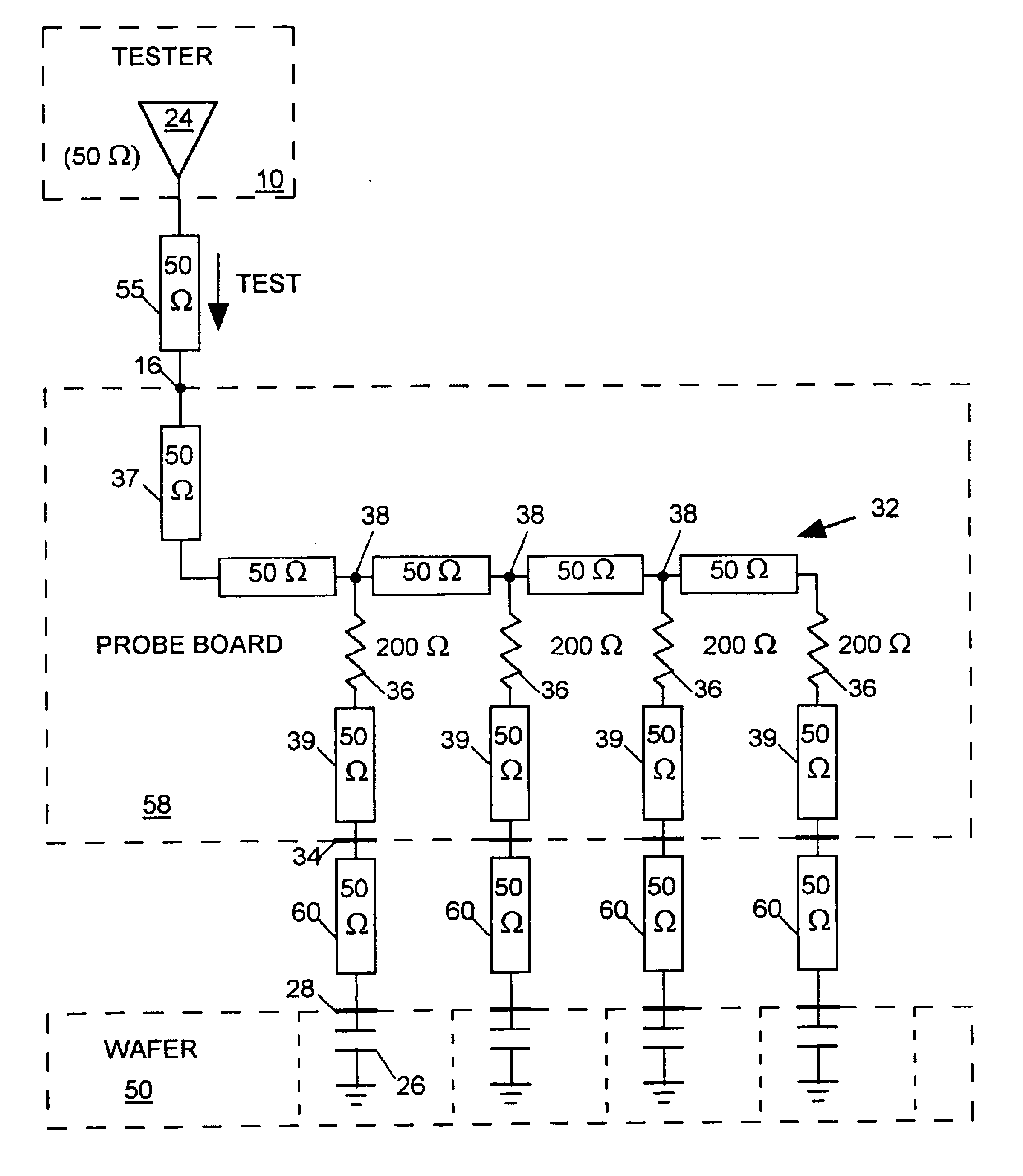
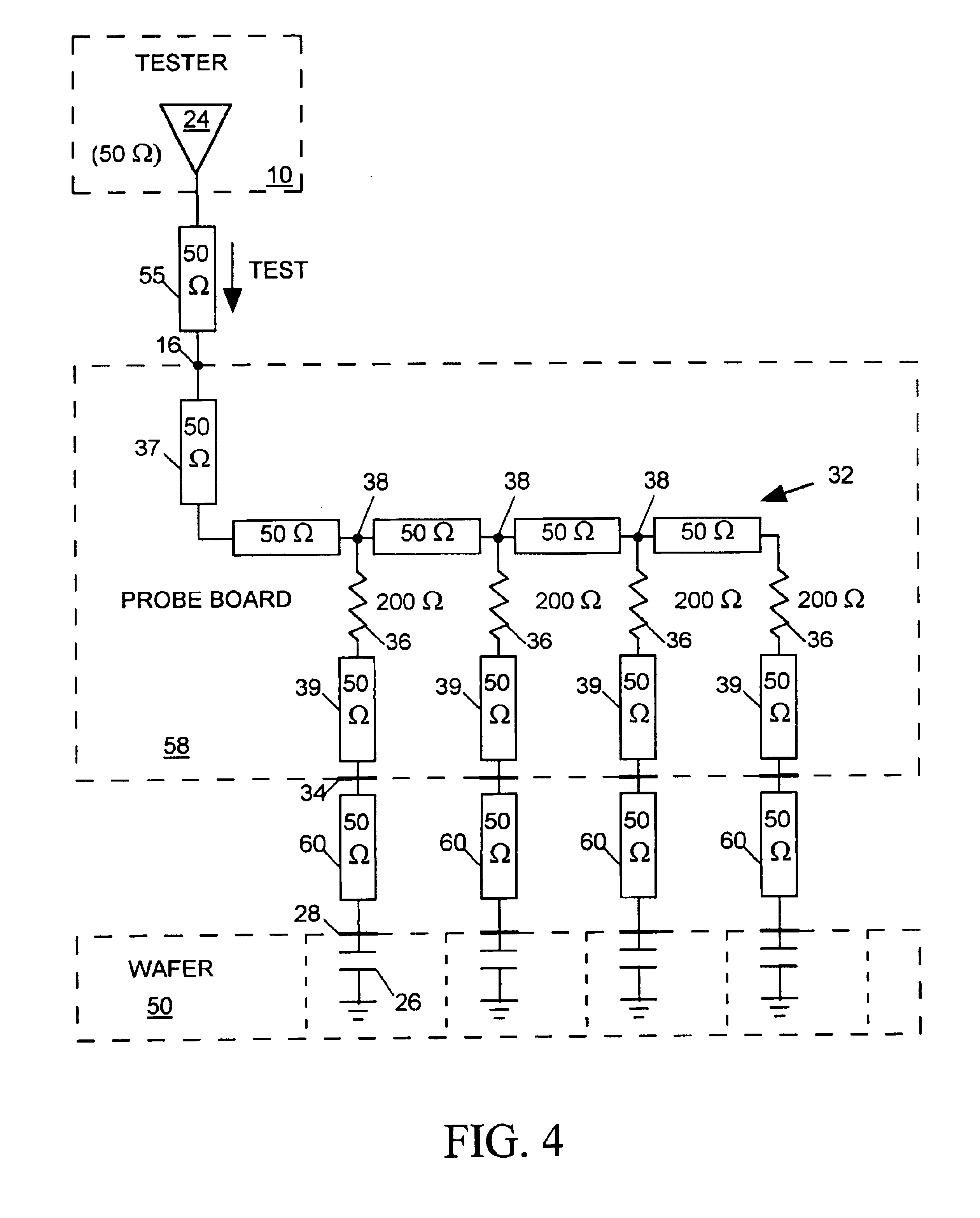
The present invention relates to an interconnect system for routing a test signal from a driver in one channel of an integrated circuit (IC) tester to more than one IC input / output (I / O) pad. The specification below describes one or more exemplary embodiments and / or applications of the invention considered by the applicant(s) to be the best modes of practicing the invention.

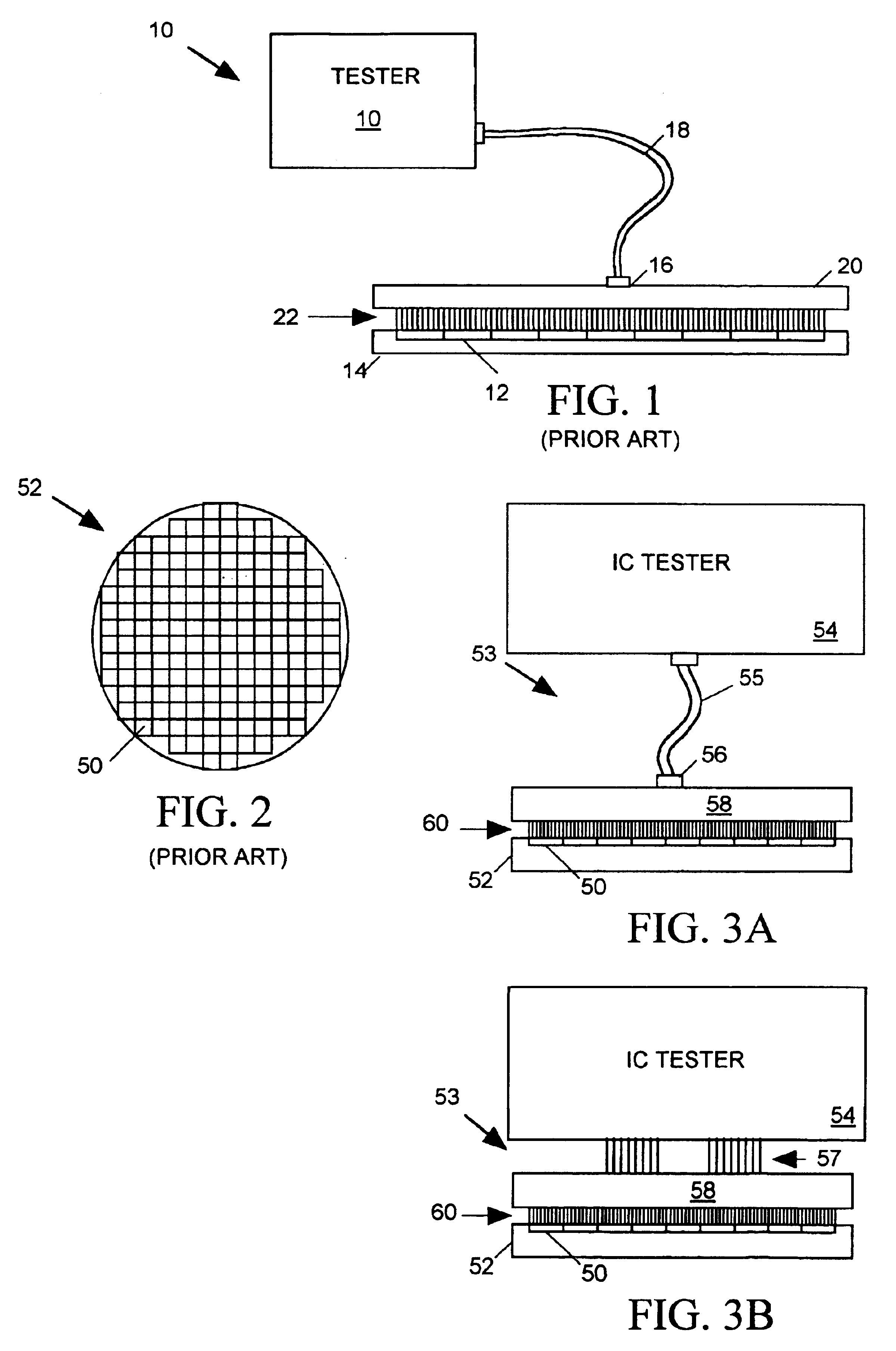
As illustrated in FIG. 2, an integrated circuit (IC) manufacturer initially forms an array of ICs 50 on a semiconductor wafer 52. The wafer is thereafter cut to separate the ICs so that they can be separately packaged or mounted on printed circuit boards. However it is advantageous to test the ICs before they are separated from one another.

FIGS. 3A and 3B are simplified side elevation views of alternative embodiments of an interconnect system 53 in accordance with the invention for providing signal paths between an integrated circuit tester 54 and the I / O pads of a set of ICs 50 formed on semiconductor wafer 52 o...


PUM


Abstract

A probe board provides signal paths between an integrated circuit (IC) tester and probes accessing terminals on the surfaces of ICs formed on a semiconductor wafer for receiving test signals form the IC tester. A branching signal path within the probe board distributes a test signal produced by one channel of the IC tester to several probes. Resistors within the branching signal path resistively isolate the probes from one another so that a fault occurring at any one IC terminal will not affect the logic state of the test signal arriving at any other IC terminal. The isolation resistors are sized relative to signal path characteristic impedances so as to substantially minimize test signal reflections at the branch points.

Description

The invention relates in general to interconnect systems for providing signal paths between an integrated circuit (IC) tester and pads on the surfaces of ICs, and in particular to a system for distributing a single test signal output of an IC tester to multiple pads on one or more ICs.DESCRIPTION OF RELATED ARTAn integrated circuit (IC) manufacturer fabricates an array of similar integrated circuits on a semiconductor wafer and then cuts the wafer to separate the ICs from one another. The ICs include pads on their upper surfaces providing points of contact for signal paths conveying IC output signals to other circuits or for receiving IC input signals from other circuits. The manufacturer may mount an IC in a package using bond wires to link the pads on the surface of the IC to package pins providing signal paths to external circuits. An IC can also be mounted directly on a printed circuit board (PCB) either by soldering pads on its surface to correspondingly arranged contact pads o...

Claims


Application Information

Patent Timeline
Patent Type & Authority Patents(United States)
IPC IPC(8): G01R1/073G01R31/319G01R31/28G01R1/067
CPCG01R1/07378G01R31/31905G01R1/06772
Inventor MILLER, CHARLES A.
Owner FORMFACTOR INC
Why Eureka
Try Eureka