Signal combiner, a signal splitter and a circuit using a combiner and a splitter

a signal combiner and combiner technology, applied in the direction of waveguides, waveguide type devices, gated amplifiers, etc., can solve the problems of amplifiers now becoming load, amplifiers losing their original contribution, and reducing the effect of failure of devices connected to the input of the signal combiner

Inactive Publication Date: 2005-01-18
COMMSCOPE TECH LLC
View PDF11 Cites 24 Cited by
  • Summary
  • Abstract
  • Description
  • Claims
  • Application Information

AI Technical Summary

Benefits of technology

By providing an input impedance transforming device, the effect of failure of a device connected to an input of the signal combiner can be reduced or alleviated.
Advantageously the switching means associated with one or more of the impedance transforming devices is arranged to connect the input of the associated impedance transforming device to ground. The advantage of this is that a switching mean does not have to be rated to handle the full amount of power which might be provided to the signal input path. For example, if the combiner was used to combine the outputs of several RF amplifiers, each rated at several hundred watts, the switch itself is not involved in connecting the output of the amplifier to an input of the signal combiner, and therefore does not have to be rated to handle several hundred watts of power and neither can it degrade the signal path. The switch merely serves to ground the input of the impedance transforming device when the amplifier is switched off or in a fault mode.

Problems solved by technology

However, should one amplifier fail, then the loss of output power is many times greater than the original contribution of that amplifier.
This is due to the fact that not only is the contribution from that amplifier lost, but the amplifier can now become a load and the power from the other amplifiers is now wasted as it flows through the output impedance of the amplifier plus the balancing loads present as part of the combiner.
The balancing loads therefore need to be adequately rated to cope with the possibility of amplifier failure and hence can become very large, possibly needing to be rated at several hundred watts in some cases.

Method used


Image

  • Signal combiner, a signal splitter and a circuit using a combiner and a splitter
  • Signal combiner, a signal splitter and a circuit using a combiner and a splitter
  • Signal combiner, a signal splitter and a circuit using a combiner and a splitter

Examples


Embodiment Construction

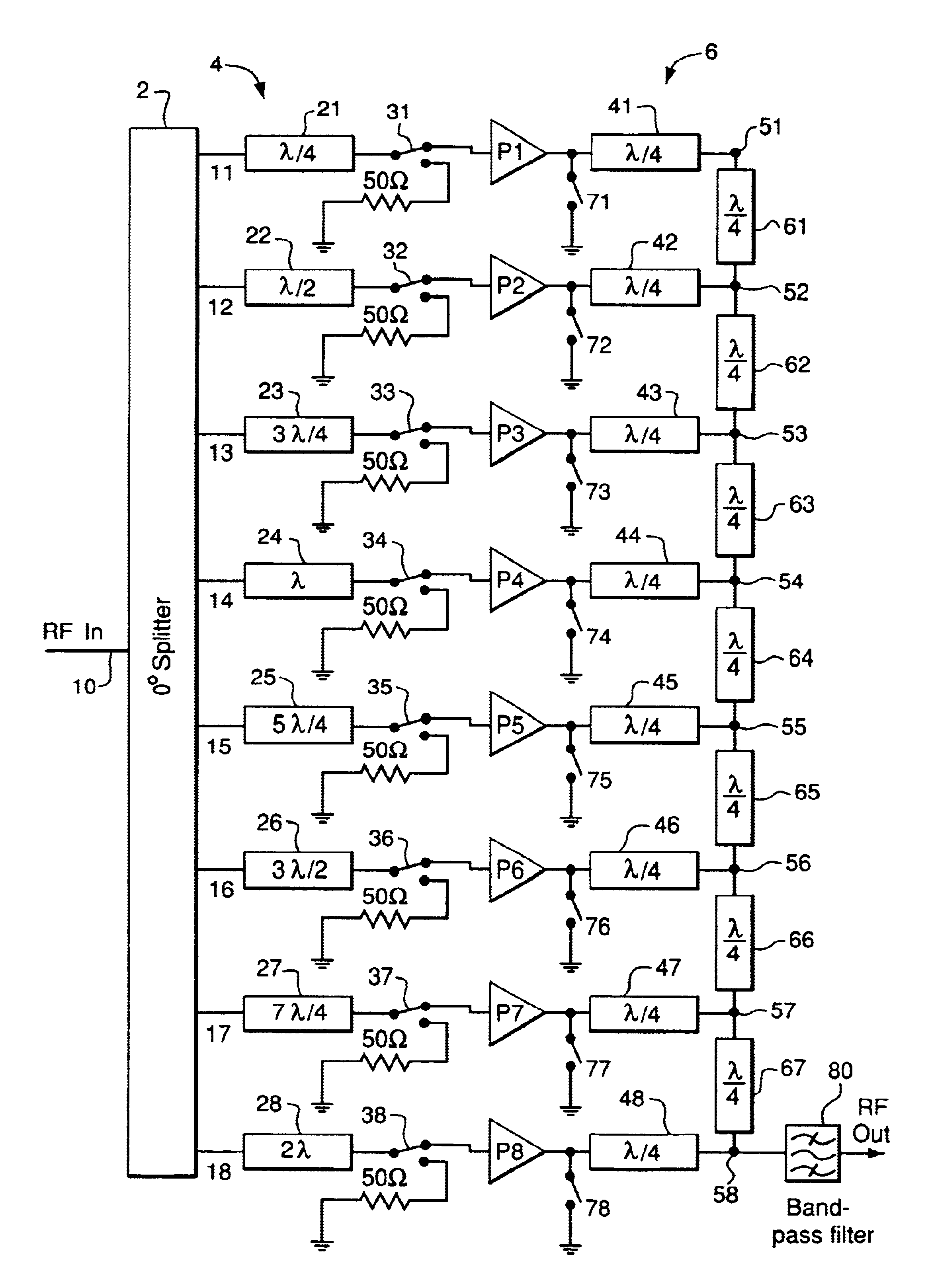
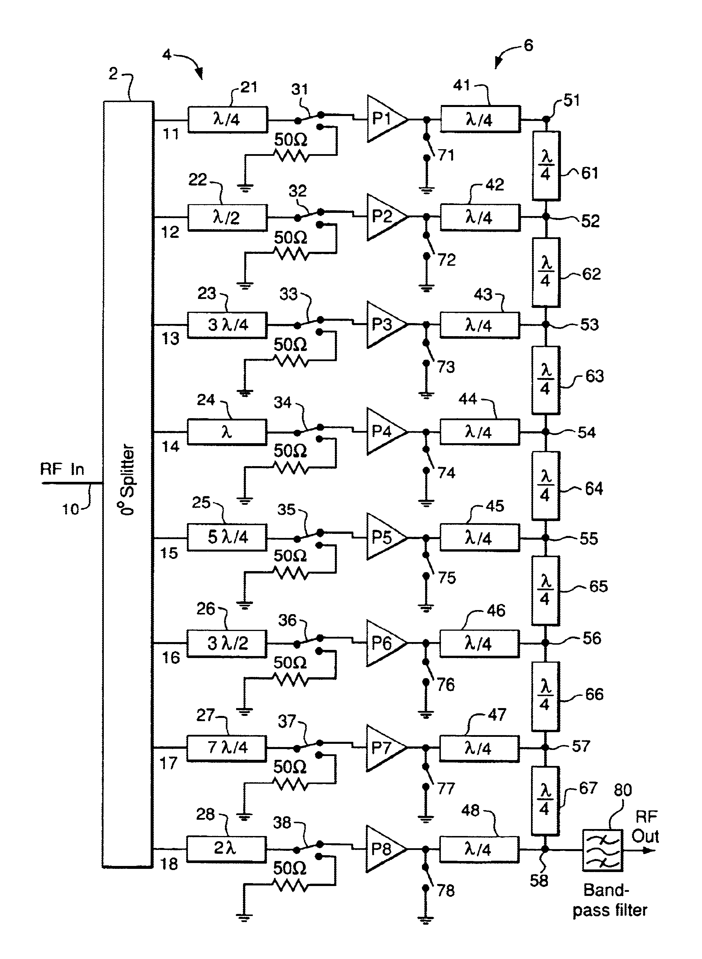
The arrangement shown in the accompanying FIGURE comprises a eight way 0° splitter 2, a phase compensation section indicated generally as 4, eight power amplifiers P1 to P8 and an eight way combiner indicated generally as 6. The circuit is designed to amplify an RF input having a carrier frequency F0 which has a wave length δ0 in a transmission line. The splitter 2 accepts an RF signal at its input 10 and splits this equally in amplitude and without introducing phase shifts between its eight outputs 11 to 18. The first output is connected to a first delay line 21 introducing a phase delay of λ4.

The second output 12 is connected to a delay line 22 introducing an delay of 2⁢λ4.

The third output 23 is connected to a third delay line 23 introducing a delay of 3⁢λ4,

and so on up to the 8th output which is connected to a delay line 28 introducing a delay of 8⁢λ4.

The output of each delay line can then be connected to an associated amplifier via a switch. Thus the output of the first delay li...


PUM


Abstract

A circuit is provided where impedance converters (41-48) are provided such that active components (P1 to P8) can be switched off without power from the other active components leaking away through those components which are switched off.

Description

FIELD OF THE INVENTIONThe present invention relates to a signal combiner, a signal splitter and to a circuit using these components.BACKGROUND OF THE INVENTIONIt is known to combine the outputs of a number of devices, such as high power amplifiers. This can be advantageous as it may deliver a method of obtaining higher output powers than might otherwise conveniently be obtainable, for example in a radio base station, or it may enable efficiencies of amplifiers to be increased by running a plurality of amplifiers of different power outputs in combination in order to achieve a desired power output. There may also be other instances in which it is desirable to combine the outputs of electronic devices.Combiners are known. For example a Wilkinson Combiner System will work acceptably to combine the outputs of a plurality of amplifiers provided that all of the amplifiers are operating. However, should one amplifier fail, then the loss of output power is many times greater than the origina...

Claims


Application Information

Patent Timeline
Patent Type & Authority Patents(United States)
IPC IPC(8): H03F1/02H03F1/52H03F3/72H03F3/60
CPCH03F1/0288H03F3/72H03F3/602H03F1/526
Inventor KENINGTON, PETER
Owner COMMSCOPE TECH LLC
Why Eureka
Try Eureka