High-frequency composite switch module and mobile communication device using the same

a composite switch module and high-frequency technology, applied in the field of high-frequency circuit modules, can solve the problems complex circuit structure, and inability to meet the needs of large number of components, and achieve the effects of low signal loss, reduced size and simplified

Inactive Publication Date: 2006-02-14
PANASONIC CORP
View PDF11 Cites 16 Cited by
  • Summary
  • Abstract
  • Description
  • Claims
  • Application Information

AI Technical Summary

Benefits of technology

[0013]It is an object of this invention to provide a small, simple, low-priced, and highly efficient high frequency composite switch module for use in a mobile communication device. In this high frequency composite switch module, high frequency circuits such as a power amplifier, a circuit that functions as a transmitter / receiver switching circuit, a band pass filter for reception and the like are integrated into one body.
[0018]With the module composed as described, the transmission signal and the reception signal in the transmitter circuit and the receiver circuit are reflected at an entry port of the respective other circuit. Therefore, switching operation for the transmission and reception signals is made equivalently. In other words, the high frequency circuit section can be downsized and simplified, since it does not require a transmitter / receiver switching circuit such as the conventional one, and thereby realizing a reduction in cost as well as low loss in handling the signals. Also, since the amplifier and the peripheral circuits are integrated into one chip, the transmission signal lines can be shortened, and loss of the transmission signals can be reduced.
[0022]In addition, at least one of an impedance matching circuit, a power supply unit and a phase shifting circuit for each of the communication systems is formed inside a multilayer board which comprises a conductor layer and a dielectric layer. Furthermore, at least one of the IC chip and a SAW filter corresponding to each of the communication systems is mounted on an outer layer of the multilayer board. The module is thus downsized and simplified, and thereby this module of low signal loss can be supplied at low price.

Problems solved by technology

Consequently, a scale of the circuit becomes inevitably large, the circuit structure becomes complicated, and a large number of components also become necessary.

Method used


Image

  • High-frequency composite switch module and mobile communication device using the same
  • High-frequency composite switch module and mobile communication device using the same
  • High-frequency composite switch module and mobile communication device using the same

Examples


first exemplary embodiment

(First Exemplary Embodiment)

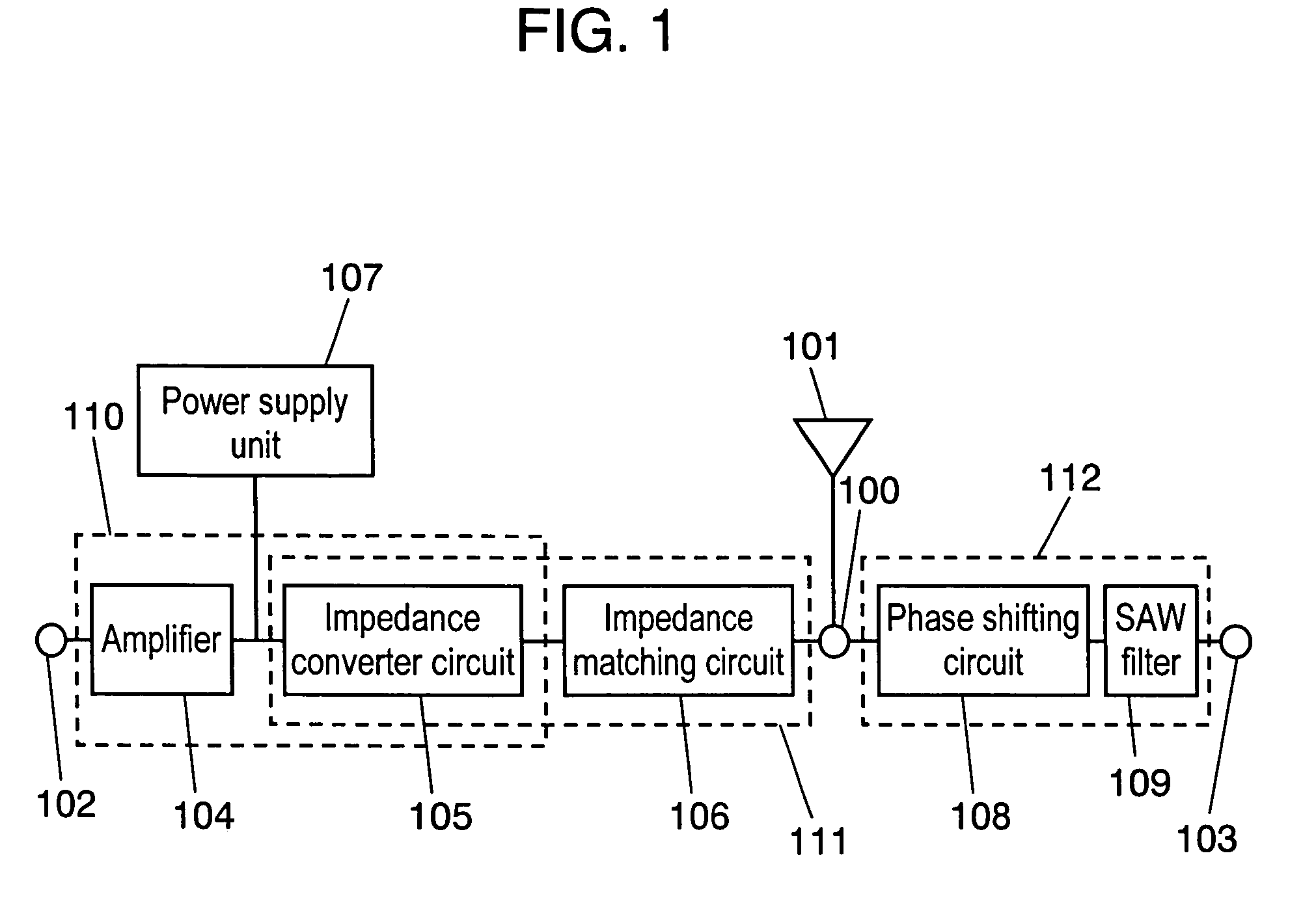
[0038]FIG. 1 is a block diagram of a high frequency composite switch module according to the first exemplary embodiment of this invention.

[0039]In this module, amplifier 104 and transmitter-side impedance converter 111 are connected between transmission terminal 102 and common terminal 100 in a transmitter circuit, as shown in FIG. 1. Power supply unit 107 is connected between amplifier 104 and transmitter-side impedance converter 111.

[0040]Transmitter-side impedance converter 111 comprises impedance converter circuit 105 and impedance matching circuit 106 in order to pass and reflect transmission signal and reception signal respectively to the maximum extent possible. In this embodiment, amplifier 104 and impedance converter circuit 105 are integrated into one IC chip 110.

[0041]In a receiver circuit, receiver-side impedance converter 112 is connected between common terminal 100 and receiving terminal 103. Receiver-side impedance converter 112 comprises p...

second exemplary embodiment

(Second Exemplary Embodiment)

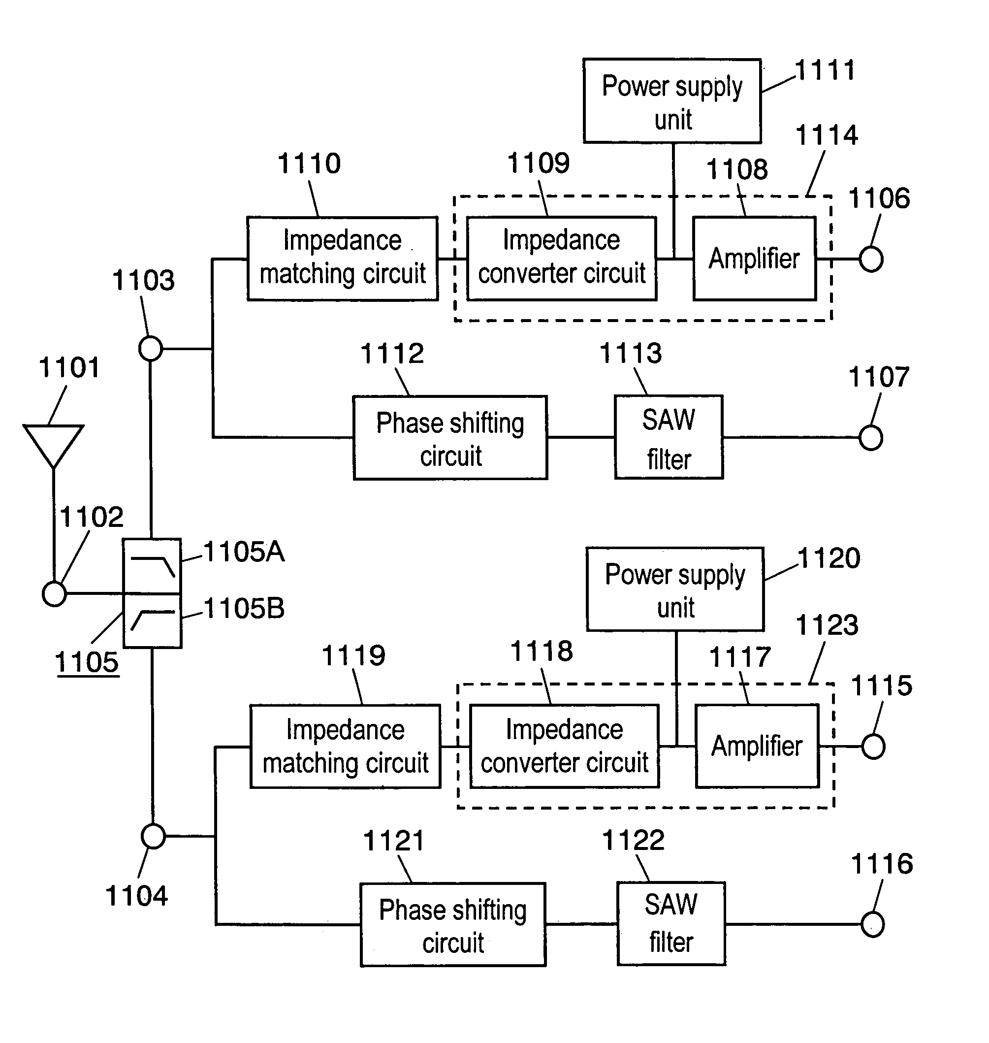
[0070]FIG. 11 is a block diagram of a high frequency composite switch module according to the second exemplary embodiment of the present invention.

[0071]The module shown in FIG. 11 enables transmission and reception through two different communication systems. The module has wave splitter circuit 1105. Wave splitter circuit 1105 has common terminal 1102 to be connected to an antenna, first terminal 1103 and second terminal 1104. Each of the first and the second terminals is connected with both a transmitter circuit and a receiver circuit in the same manner as the first exemplary embodiment.

[0072]A first transmitter circuit comprising first amplifier 1108, first power supply unit 1111, first impedance converter circuit 1109 and first impedance matching circuit 1110 is connected between first terminal 1103 and first transmission terminals 1106. Here, first impedance converter circuit 1109 and first impedance matching circuit 1110 constitute a first transmi...


PUM


Abstract

A high frequency composite switch module for a mobile communication device, wherein high frequency circuits such as a power amplifier, a circuit functioning as a transmitter / receiver switching circuit, a surface acoustic wave (SAW) filter for reception, and the like are modularized into one unit. A transmitter circuit includes a transmitter side impedance converter comprising an impedance matching circuit and an impedance converter circuit, a power amplifier and a power supply unit. A receiver circuit includes a receiver-side impedance converter comprising a phase shifting circuit and a SAW filter. The power amplifier and the impedance converter circuit are integrated into one IC chip. At least one of the matching circuit, the power supply unit and the phase shifting circuit is formed inside a multilayer board comprised of a conductor layer and a dielectric layer. The IC chip and the SAW filter are also mounted on the multilayer board.

Description

[0001]This application is a U.S. National Phase applicationn of PCT International application PCT / JP02 / 09259.TECHNICAL FIELD[0002]The present invention relates to a high frequency circuit module adapted for use in a mobile communication device such as a portable phone.BACKGROUND ART[0003]With widespread use of mobile telecommunications such as portable phones, there is an upward trend in use of mobile communication devices that have facilities to use two different communication systems such as the dual-band cellular telephone system.[0004]Any such telecommunication device hitherto often shares an antenna for both of the two communication systems. The device requires two channels of transmitter circuit and receiver circuit independently for the respective communication systems. Each of them is selected with a switch for making a communication. In general, a high frequency section in any of these transmitter circuits comprises a power amplifier, a low pass filter, and the like. A high...

Claims


Application Information

Patent Timeline
Patent Type & Authority Patents(United States)
IPC IPC(8): H03F1/14H01L25/18H01L25/04H04B1/44H04B1/52
CPCH04B1/52H04B1/44
Inventor KUSHITANI, HIROSHISATOH, YUKI
Owner PANASONIC CORP
Why Eureka
Try Eureka