Liquid crystal display device and method for driving the same

a display device and liquid crystal technology, applied in static indicating devices, non-linear optics, instruments, etc., can solve the problems of video signal distortion, video signal distortion, and video signal distortion of data lines, so as to reduce cross-talk, improve screen display quality, and prevent signal coupling

Inactive Publication Date: 2005-01-25
LG DISPLAY CO LTD
View PDF13 Cites 15 Cited by
  • Summary
  • Abstract
  • Description
  • Claims
  • Application Information

AI Technical Summary

Benefits of technology

An object of the present invention is to provide an LCD device and a method for driving the same that can improve the screen display quality and reduce cross talks by preventing the signal coupling between data lines.

Problems solved by technology

The parasitic capacitance causes distortion of the video signals applied to the data lines.
Therefore, if the control signals Cn become active, the video signals applied to the corresponding data line are significantly distorted.
Such a distortion of the video signals is attributable to the parasitic capacitance generated between the two data lines adjacent to a given liquid crystal capacitor.
However, reduction of the parasitic capacitance has a limit as it is closely related to an aperture rate.
Thus, the conventional LCD device and its associated driving method described above pose a problem by generating a coupling, which is attributable to a parasitic capacitance between a liquid crystal capacitor and adjacent data lines due to the video signals applied to the data lines consecutively.
In other words, when there is a difference in a screen pattern, a value of the liquid crystal capacitor is changed and the coupling voltage is changed due to the parasitic capacitance, thereby reducing the screen display quality.

Method used


Image

  • Liquid crystal display device and method for driving the same
  • Liquid crystal display device and method for driving the same
  • Liquid crystal display device and method for driving the same

Examples


first embodiment

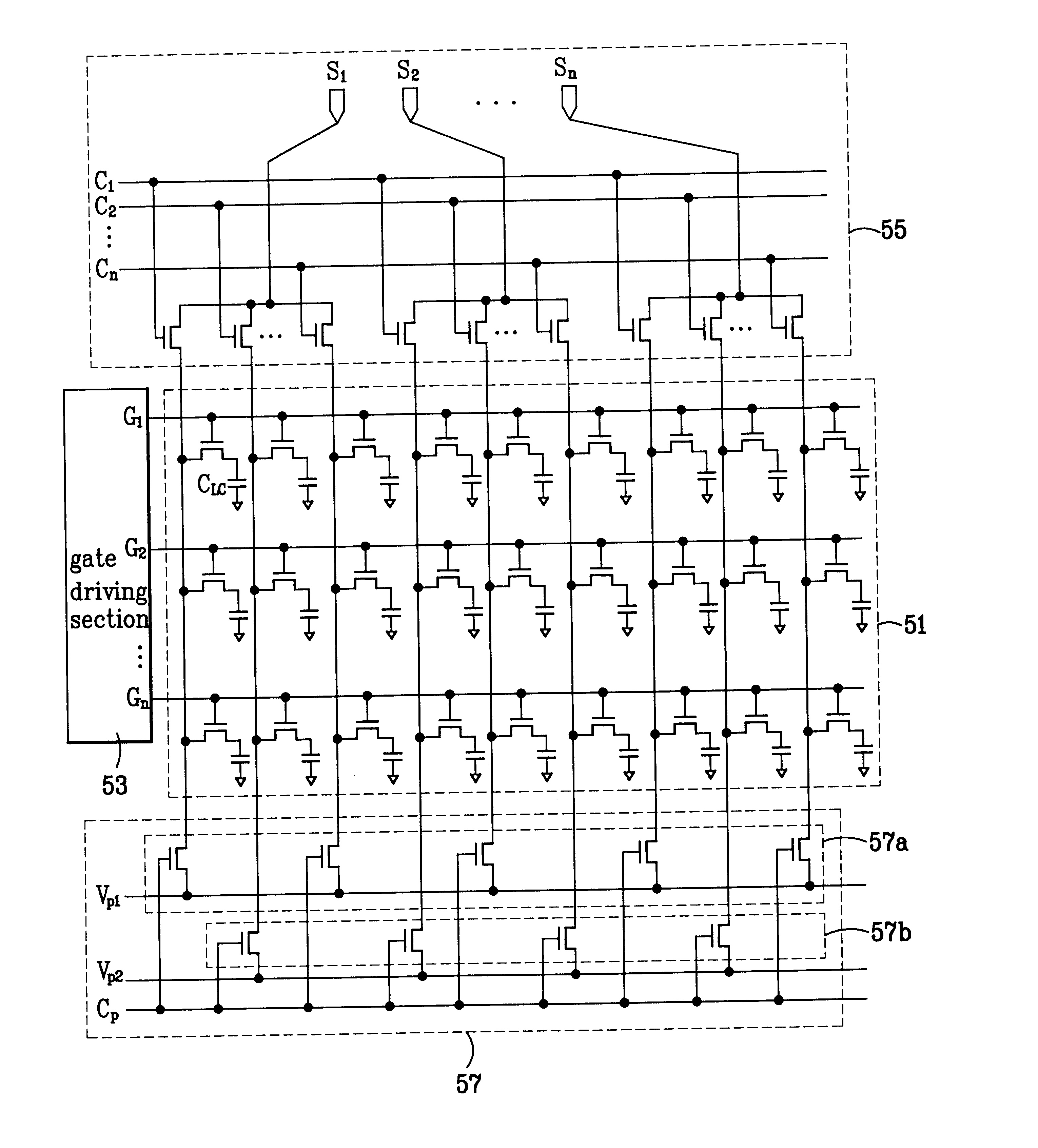
FIG. 5 is a block diagram illustrating a construction of an LCD device according to a first embodiment of the present invention.

Referring to FIG. 5, an LCD device comprises a pixel section 51 including a plurality of gate lines G1, G2, . . . , Gn and data lines D1, D2, . . . , Dn arranged to cross each other and a plurality of thin film transistors (TFTs) and liquid crystal capacitors CLC formed at each crossing point, a gate driving section 53 for applying driving signals to the gate lines in order, a source driving section 55 for applying video signals S1, S2, . . . , Sn to each set of data lines in order, and a precharge circuit section 57 for supplying different precharging voltages to adjacent data lines.

Here, the precharge circuit section 57 comprises first precharging voltage terminals Vp1, second precharging voltage terminals Vp2, a first switching section 57a for switching the voltage of the first precharging voltage terminals Vp1 with odd number data lines D1, D3, D5, . . ...

second embodiment

the invention does not require any external switches for switching voltages between the first precharging voltage terminals and the second precharging voltage terminals even if the polarities of the video signals loaded on each data line are reversed as each gate line is activated.

FIG. 6 is a block diagram illustrating a precharge circuit section of the LCD device according to a second embodiment of the present invention.

Referring to FIG. 6, the precharge circuit section 67 incudes switching sections 67_1, 67_2, . . . , 67—n connecting first switching elements 67a and second switching elements 67b to each data line. The first and second switching elements 67a and 67b have output terminals connected in common, but with different input sources.

In the odd number data lines, either the first precharging voltage Vp1 is applied through the first switching elements 67a in accordance with the first precharge control signal Cp1, or the second precharging voltage Vp2 is applied through the se...

third embodiment

The third embodiment of the present invention has a further modified construction of the precharge circuit section. The precharge circuit section according to the second embodiment employs the first switching element and the second switching element that are commonly connected to the data lines and composed of thin film transistors of an identical conductive type. In comparison, the precharging circuit section according to the third embodiment employs the first switching element and the second switching element composed of film transistors of opposite conductive types.

FIG. 9 is a block diagram illustrating a construction of the precharge circuit section of the LCD device according to the third embodiment of the present invention. FIG. 10 is a block diagram illustrating a construction of the LCD device employing the precharge circuit section in FIG. 9 according to the third embodiment of the present invention.

The precharge circuit section according to the third embodiment of the pres...


PUM

PropertyMeasurementUnit
voltageaaaaaaaaaa
voltageaaaaaaaaaa
voltageaaaaaaaaaa

Abstract

A liquid crystal display (LCD) device having a first substrate and a second substrate with liquid crystal sealed therebetween, includes a plurality of gate lines and data lines crossing each other on the first substrate; a gate driving section for driving the gate lines; a source driving section for precharging the data lines for a first time and supplying video signals to the data lines; and a precharge circuit section for precharging the data lines for a second time.

Description

The present invention claims the benefit of Korean Patent Application No. P 2000-50770 filed in Korea on Aug. 30, 2000, which is hereby incorporated by reference.BACKGROUND OF THE INVENTION1. Field of the InventionThe present invention relates to a flat display device, and in particular, to a liquid crystal display (LCD) device and a method for driving the same with enhanced screen quality and reduced cross-talk effect.2. Description of the Related ArtIn general, an LCD device is manufactured by facing two glass substrates (also called top and bottom plates) and injecting liquid crystal in the space between the two glass substrates. A data line and a gate line are arranged in a matrix form at the bottom plate to define a plurality of pixel regions. A thin film transistor and a pixel electrode are aligned in each pixel region.Provided at the top plate are a common electrode for applying a common voltage to the liquid crystal, and a color filter layer for expressing colors of red, gre...

Claims


Application Information

Patent Timeline
Patent Type & Authority Patents(United States)
IPC IPC(8): G09G3/36G02F1/133
CPCG09G3/3648G09G3/3614G09G2320/0209G09G2310/0248G02F1/133
Inventor HA, YONG MIN
Owner LG DISPLAY CO LTD
Why Eureka
Try Eureka