Method of manufacturing a solid-state imaging device

a solid-state imaging and manufacturing method technology, applied in semiconductor devices, radio-controlled devices, electrical apparatuses, etc., can solve the problems of reduced transfer efficiency and transfer charge quantity, reduced resolution of conventional imaging devices, and reduced sensitivity when transparent films are thick, so as to achieve superior sensitivity or resolution, reduce the effect of transfer efficiency or transfer charge quantity

Inactive Publication Date: 2005-02-01
NEC ELECTRONICS CORP
View PDF15 Cites 16 Cited by
  • Summary
  • Abstract
  • Description
  • Claims
  • Application Information

AI Technical Summary

Benefits of technology

It is therefore an object of the present invention to provide a frame transfer-type or a full frame transfer-type solid imaging device and method of manufacturing the same, which is superior in sensitivity or resolution without reducing the transfer efficiency or the transfer charge quantity.

Problems solved by technology

However, several problems have been encountered in the conventional solid imaging device: the sensitivity is reduced when the transparent film is thick, and the transfer efficiency and the quantity of the transfer charge are reduced when the transparent film is thin.
The resolution of the conventional imaging device is also not satisfactory.
However, when the thickness of the transparent film is increased, a part of the light incident to the transparent film is diffused, and the transparency of the transparent electrode decreases so that the sensitivity of the imaging device is reduced.
If the thin transparent electrode is used in order to increase the sensitivity, the wiring resistance increases, which results in causing a problem of the pulse rounding, and in decreasing the transfer efficiency and the transfer charge quantity.
Furthermore, when the structure shown in FIG. 7 is considered, light incident to the periphery of the channel stop region through the transparent electrode is distributed to both of the photoelectric conversion regions of the channel stop region to cause photoelectric conversion, which results in the reduction of the resolution of the imaging device.

Method used


Image

  • Method of manufacturing a solid-state imaging device
  • Method of manufacturing a solid-state imaging device
  • Method of manufacturing a solid-state imaging device

Examples


first embodiment

[First Embodiment]

Hereinafter, the first embodiment of the present invention is described with reference to FIGS. 1 to 4.

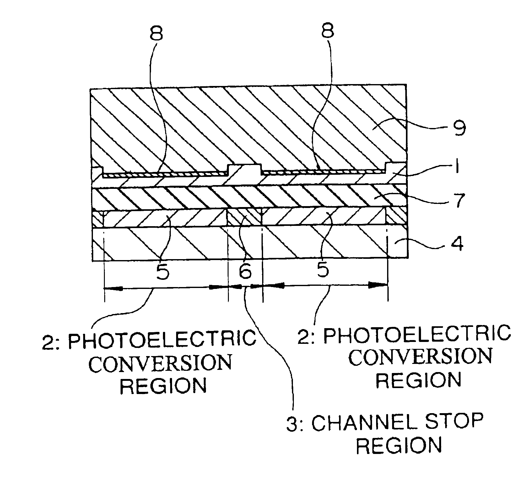
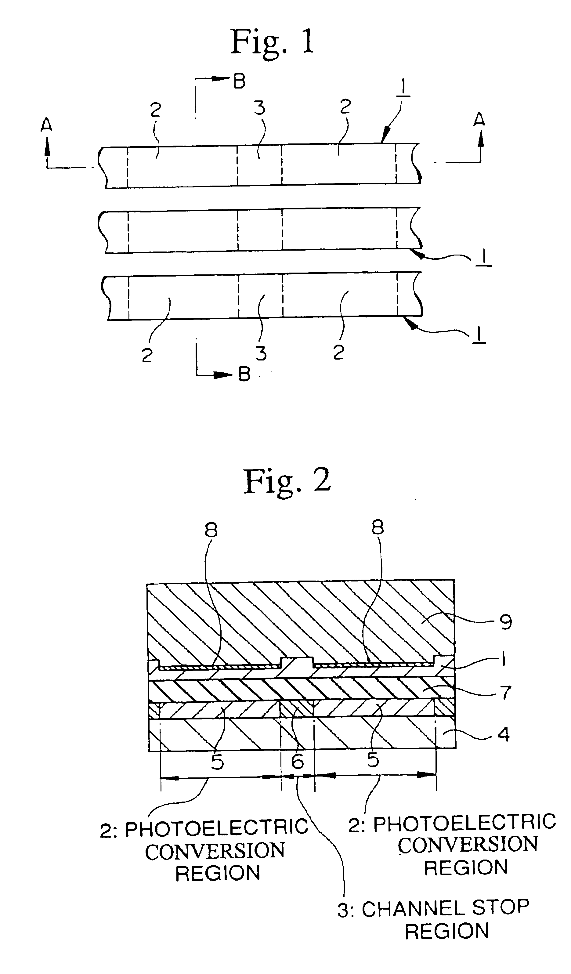
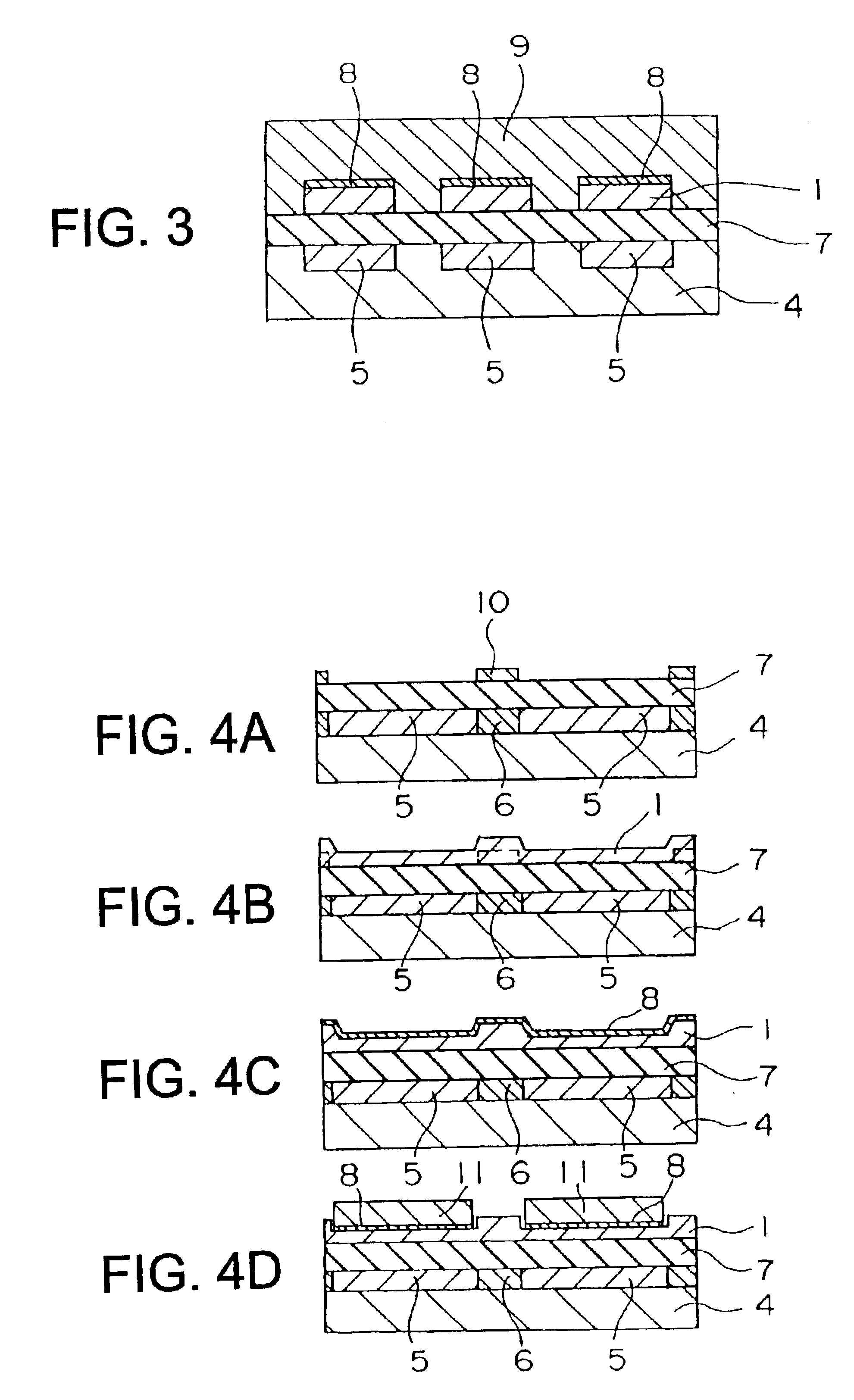
FIG. 1 is a planar view showing a structure, in particular to a structure of the light receiving portion of a CCD type solid imaging device according to the first embodiment of the present invention. FIG. 2 shows a cross-sectional diagram (along line A—A in FIG. 1), FIG. 3 shows a cross-sectional diagram (along line B—B in FIG. 1), and FIGS. 4A to 4D are cross-sectional diagrams showing the manufacturing process of the CCD type solid imaging device according to the first embodiment of the present invention.

As shown in FIG. 1, the light receiving portion of the CCD-type imaging device of the present invention comprises a plurality of transparent electrodes 1 extending to the lateral direction, a plurality of photoelectric conversion regions 2 along each transparent electrode, and a plurality of channel stop regions 3, each of which separates respective two photoele...

second embodiment

[Second Embodiment]

Hereinafter, the second embodiment of the present invention is described with reference to FIGS. 5 and 6A to 6D.

FIG. 5 is a cross-sectional diagram showing the frame transfer-type CCD-type solid imaging device according to the second embodiment of the present invention. FIGS. 6A to 6D are cross-sectional diagrams showing the manufacturing process of the CCD type solid imaging device according to the second embodiment of the present invention. Since the planar view and the cross-sectional view along the lateral direction of the transparent electrode are similar to those of the first embodiment, their illustrations are omitted. In FIGS. 5 and 6, the same components as those in FIGS. 2 and 4 are denoted by the same numerals.

In the CCD-type solid imaging device according to the second embodiment shown in FIG. 5, an N-type region 5 which constitutes the photoelectric conversion region 2 and a P+-type region 6 which constitutes the channel stop region 6 are formed on th...


PUM


Abstract

A frame transfer-type solid imaging device is provided, which can be operated without reducing the transfer efficiency or the transfer charge quantity. A plurality of N-type regions 5 constituting photoelectric conversion regions and a plurality of P+-type regions 6 constituting channel stop regions are formed on a P-type silicon substrate 4, and a transparent electrode 1 is further formed through an insulating film 7 on the substrate 4. The thickness of the transparent electrode at a portion above the photoelectric conversion region is made thinner than the thickness of the other part of the transparent electrode 1, and an antireflection film 8 is formed above the photoelectric conversion region 2.

Description

BACKGROUND OF THE INVENTION1. Field of the InventionThe present invention relates to a solid imaging device and a method of manufacturing the same, and particularly relates to a frame transfer or a full frame transfer-type solid imaging device, which is provided with the improved sensitivity and resolution without reducing the transfer efficiency or the transfer charge.2. Background ArtWhen CCD type solid imaging devices are classified by their operation mode, there are two systems: one is an interline transfer system and another one is a frame transfer system (or a full-frame transfer system). In the solid imaging device operated by the interline transfer system, each pixel is constructed by a PN junction, and light is incident on the N-type region through the insulating film formed on the region. A vertical CCD resistor is formed adjacent to each pixel in sequence, and the signal charge accumulated on the light receiving portion is transferred to the vertical CCD resistor. The con...

Claims


Application Information

Patent Timeline
Patent Type & Authority Patents(United States)
IPC IPC(8): H01L27/148
CPCH01L27/14625H01L27/1485H01L27/14687H01L27/14685H01L27/148
Inventor MURAKAMI, ICHIRONAKASHIBA, YASUTAKA
Owner NEC ELECTRONICS CORP
Why Eureka
Try Eureka