
Electrode configuration in a MEMS switch

a technology of mems switch and configuration, applied in the field of microelectromechanical systems, can solve the problems of significant resistance between protuberances b, speed limitation precludes the application of mems switches in certain cases, and the general speed of mems switches is generally much slower than solid-state switches

Inactive Publication Date: 2005-02-01
INTEL CORP
View PDF17 Cites 41 Cited by
  • Summary
  • Abstract
  • Description
  • Claims
  • Application Information

AI Technical Summary

Problems solved by technology

However, MEMS switches are generally much slower than solid-state switches.
This speed limitation precludes applying MEMS switches in certain technologies, such as wireless communications, where sub-microsecond switching is required.
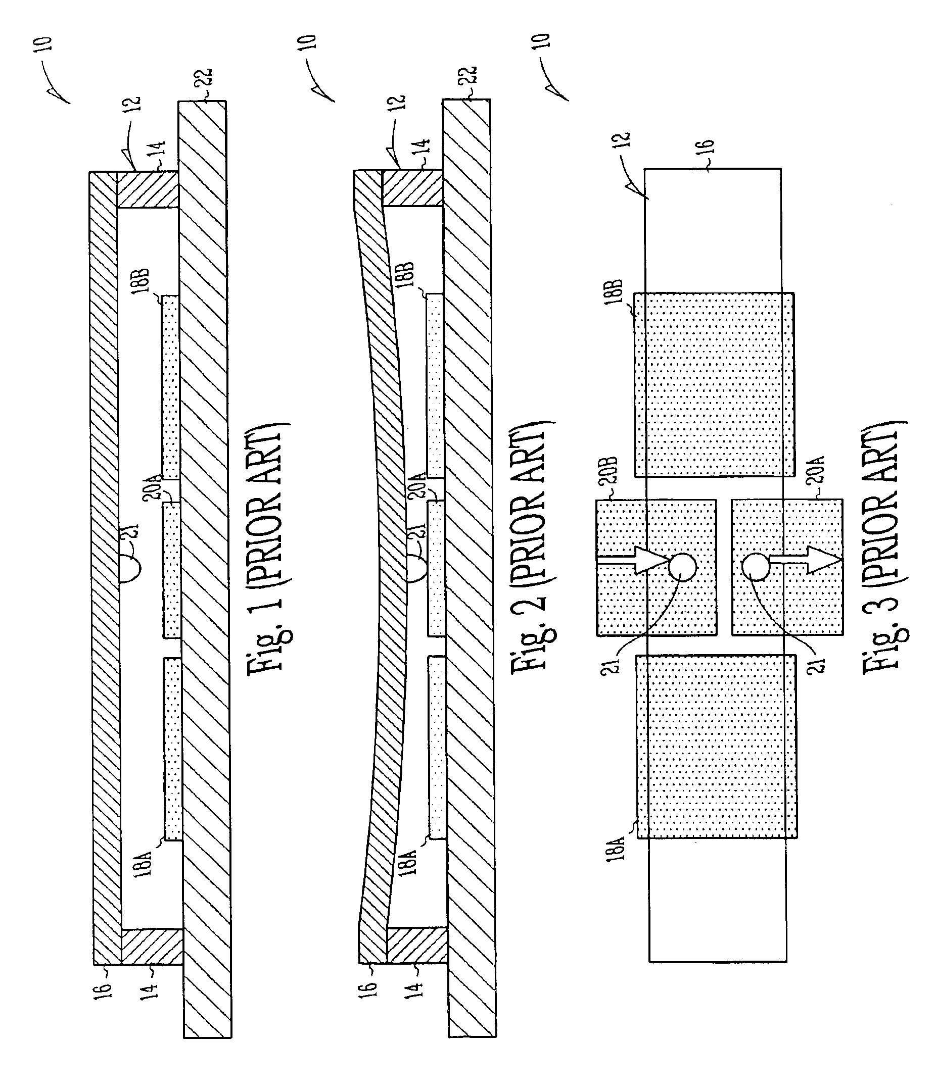
One drawback associated with MEMS switch 10 is that there is significant resistance between protuberances 21 on beam 12 and the pads that form signal contacts 20A, 20B.
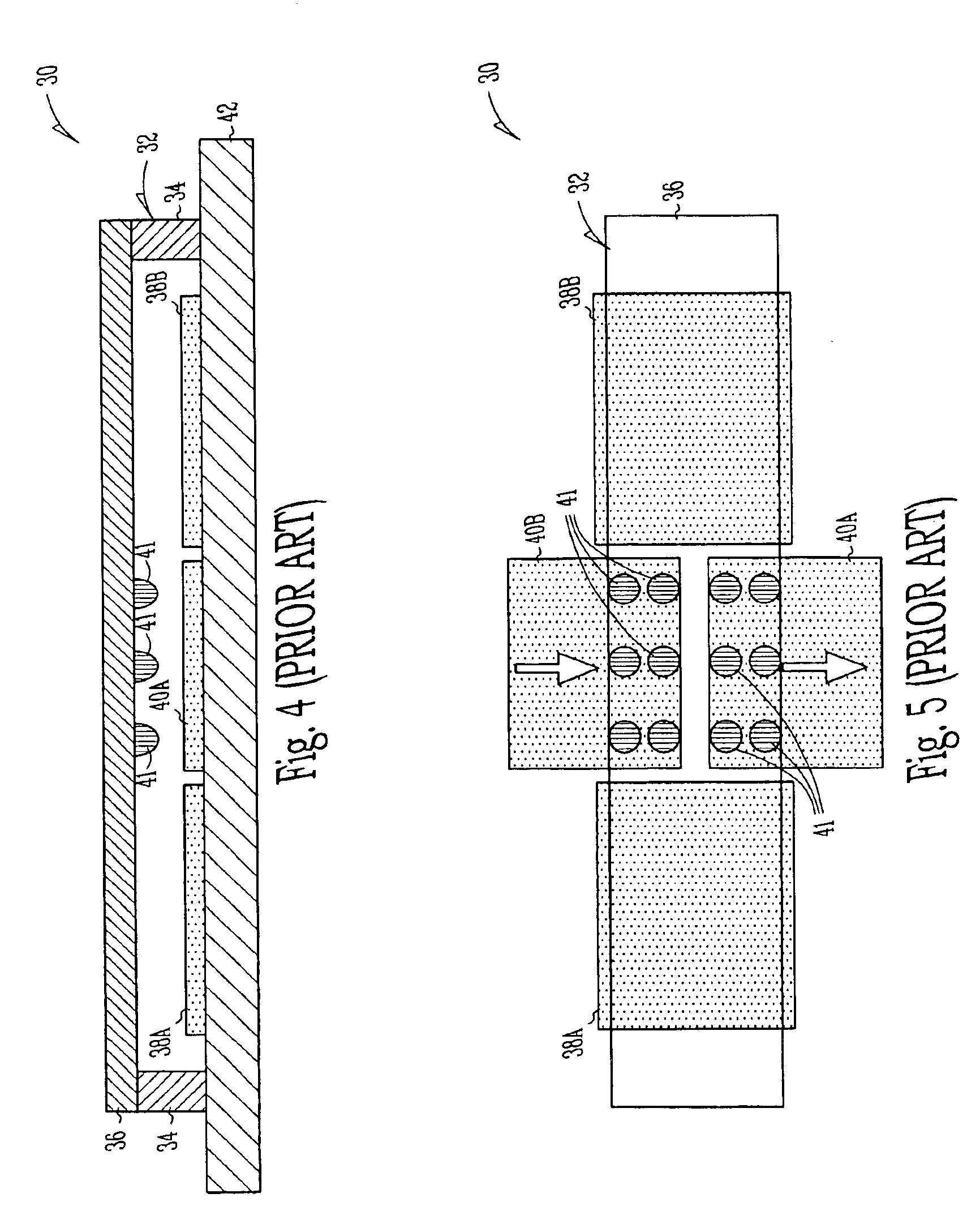
The drawback with adding additional protuberances is that only a few of the protuberances 41 actually establish good electrical contact with signal contacts 20A, 20B.
Therefore, MEMS switch 30 still has considerable insertion loss.
Increased actuation voltage is undesirable because more equipment and / or power are required to operate MEMS switch 50.
The necessary additional equipment and power are especially problematic when MEMS switches are used in portable electronic devices powered by batteries.

Method used


Image

  • Electrode configuration in a MEMS switch
  • Electrode configuration in a MEMS switch
  • Electrode configuration in a MEMS switch

Examples


Embodiment Construction

In the following detailed description reference is made to the accompanying drawings in which is shown by way of illustration specific embodiments. These embodiments are described in sufficient detail to enable those skilled in the art to practice the embodiments of invention. Other embodiments may be utilized and / or changes made to the illustrated embodiments.

FIGS. 8 and 9 show a MEMS switch 70. MEMS switch 70 includes a substrate 72 with an upper surface 74. The substrate 72 may be part of a chip or any other electronic device. An actuation electrode 76 and a signal contact 78 are formed on the upper surface 74 of substrate 72. The actuation electrode 76 and signal contact 78 are electrically connected with other electronic components via conducting traces in the substrate 72, or through other conventional means.

Switch 70 further includes a bridge beam 80 having a flexible portion 82 supported at both ends by structural portions 84. It should be noted that in alternative embodimen...


PUM


Abstract

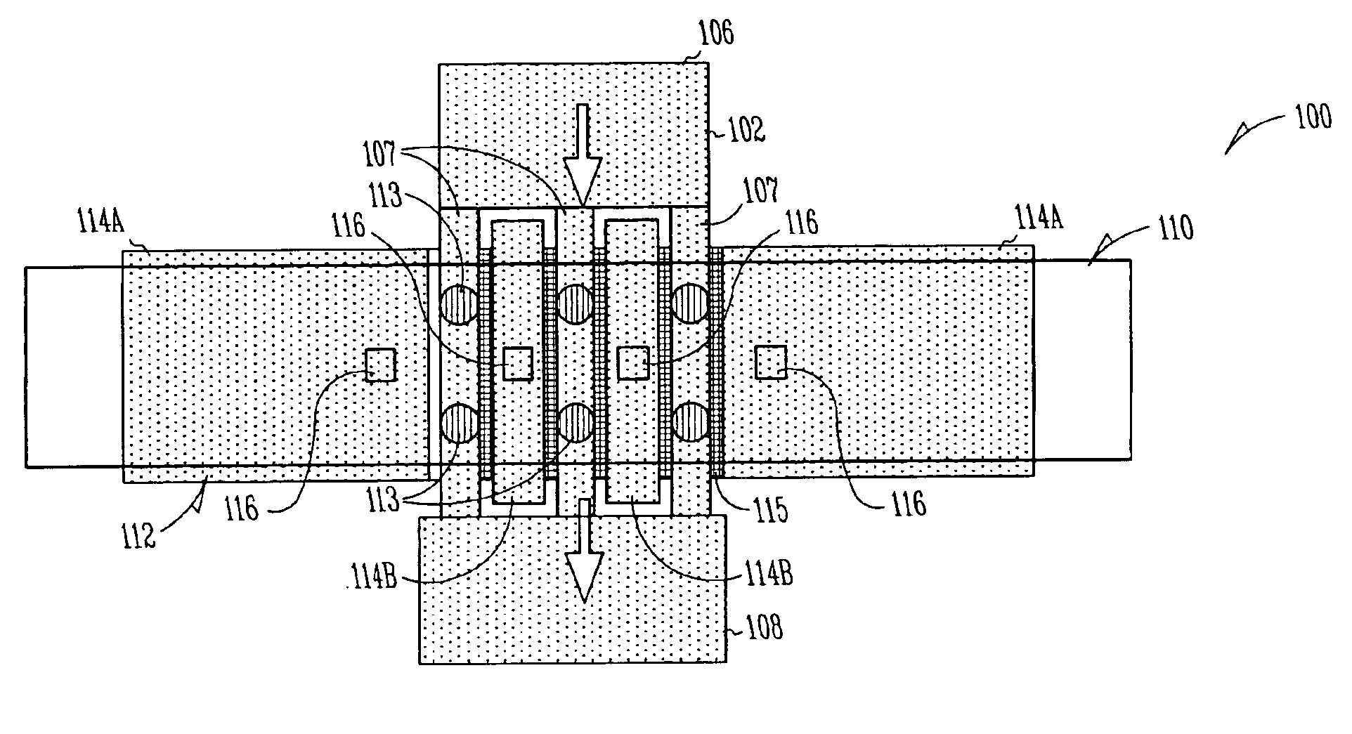
A microelectromechanical system (MEMS) switch that includes a signal contact, an actuation electrode and a beam that engages the signal contact when a voltage is applied to the actuation electrode. The signal contact includes a first portion and a second portion. The actuation electrode is positioned between the first and second portions of the signal contact.

Description

TECHNICAL FIELDMicroelectromechanical systems (MEMS), and in particular to MEMS switches that have an improved electrode configuration.BACKGROUNDA microelectromechanical system (MEMS) is a microdevice that integrates mechanical and electrical elements on a common substrate using microfabrication technology. The electrical elements are formed using known integrated circuit fabrication techniques, while the mechanical elements are fabricated using lithographic techniques that selectively micromachine portions of a substrate. Additional layers are often added to the substrate and then micromachined until the MEMS device is in a desired configuration. MEMS devices include actuators, sensors, switches, accelerometers, and modulators.MEMS switches have intrinsic advantages over conventional solid-state counterparts such as field-effect transistor switches. The advantages include low insertion loss and excellent isolation. However, MEMS switches are generally much slower than solid-state s...

Claims


Application Information

Patent Timeline
IPC IPC(8): H01H59/00B81B3/00
CPCH01H59/0009
Inventor MA, QING
Owner INTEL CORP
Learn More