Control circuit and control method for display device

a control circuit and display device technology, applied in the field of control circuits and control methods of matrix-type display devices, can solve the problems of significant flicker or waving, frame modulation system, number of frames, etc., and achieve the effect of reducing the frequency of a waveform applied to each of a plurality of column electrodes, reducing the rate, and reducing the rounding of a data voltag

Inactive Publication Date: 2005-02-01
SHARP KK
View PDF7 Cites 8 Cited by
  • Summary
  • Abstract
  • Description
  • Claims
  • Application Information

AI Technical Summary

Benefits of technology

According to the present invention, the frequency of a waveform applied to each of a plurality of column electrodes is decreased. Therefore, the rounding of a data voltage can be reduced. The waveform distortion of a scanning voltage which is induced by a data voltage also occurs at a reduced rate.
Moreover, even when input display data for different column electrodes are the same, it is possible to change the waveforms of data voltages in different timings, preventing data voltages having the same waveform from being applied to different electrodes in the same horizontal scanning period. Therefore, the amplitude of waveform distortion of a scanning voltage which is induced by the data voltage can be reduced.
As a result, it is possible to obtain a driving waveform applied to the column electrode and a driving waveform applied to the row electrode, both of which are close to the respective ideal waveforms. Therefore, the RMS value of a voltage actually applied to each pixel can be close to the ideal value, thereby preventing a reduction in display quality, such as crosstalk.
Thus, the invention described herein makes possible the advantages of providing a control circuit and a control method for use in a display device in which crosstalk or the like can be reduced and thus display quality is improved in gray scale display.

Problems solved by technology

The frame modulation system, however, poses the following problem.
The increased number of frames leads to a significant flicker or waving in a display.
For this reason, when the frame modulation system is used for a liquid crystal panel having high speed response, for example, the problem becomes more significant.
For this reason, the frequency of the data voltage signal becomes higher, resulting in the significant rounding of the data voltage signal caused by electrode resistance and liquid crystal capacity and the wave-form distortion of a scanning voltage induced by a data voltage.
In this case, a root-mean-square (RMS) value of voltage whose value is different from the RMS value of the original voltage is applied to liquid crystal, which leads to a reduction in display quality, such as crosstalk.
The above-described problem on the pulse width modulation system still remains in the method disclosed in the above-described Japanese Laid-Open Publication No. 2-1812 where gray scale obtained by the pulse width modulation is further subjected to the frame modulation.
The higher frequency the driving waveform applied to the column electrode has, the more number of times the waveform changes, resulting in an increased rate of waveform distortion.
This leads to a reduction in display quality, such as crosstalk.

Method used


Image

  • Control circuit and control method for display device
  • Control circuit and control method for display device
  • Control circuit and control method for display device

Examples


example 1

(Example 1)

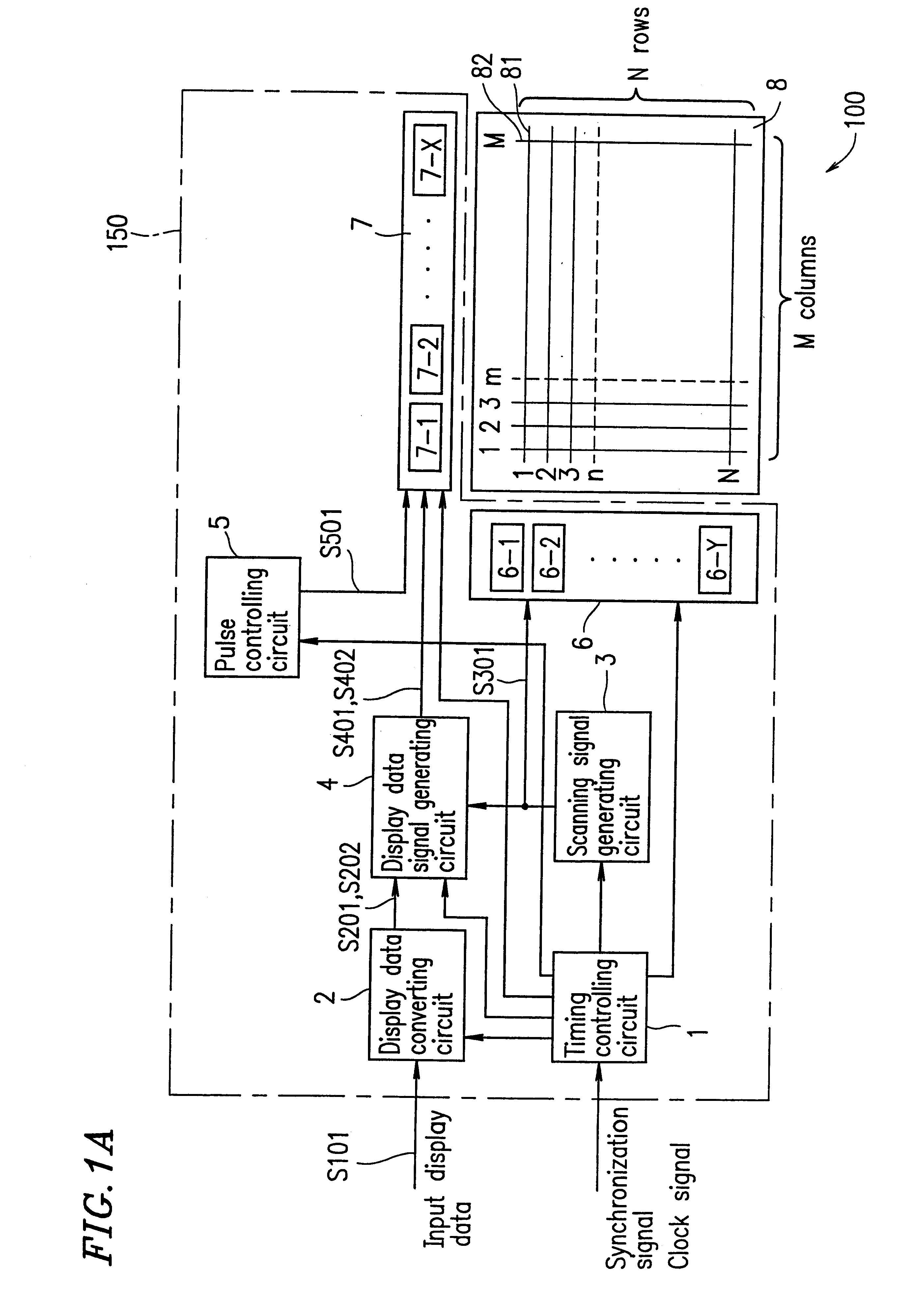
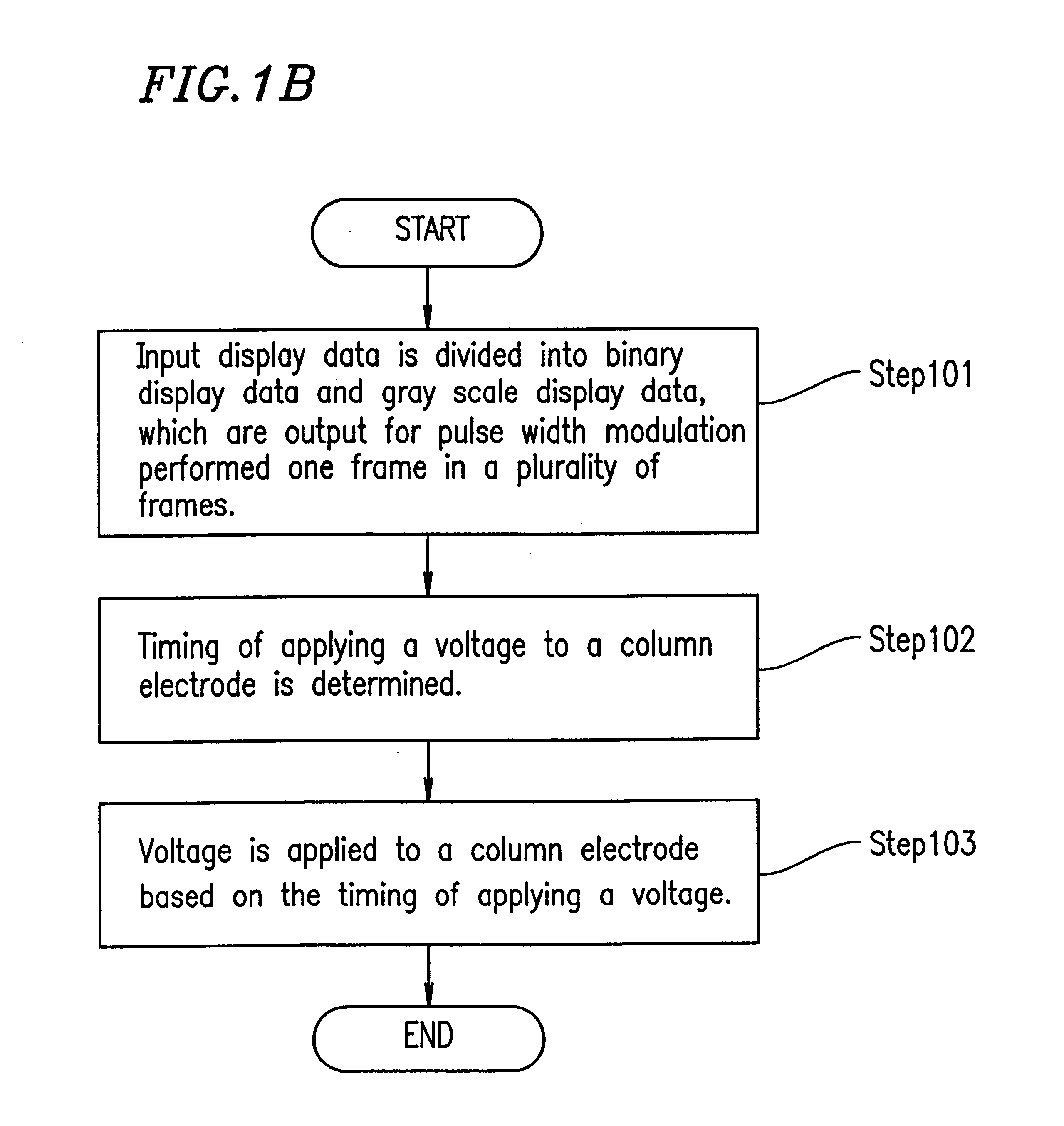
FIG. 1A shows an example configuration of a display device 100 according to Example 1 of the present invention. FIG. 1B is a flowchart illustrating the operation of the display device 100.

As shown in FIG. 1A, the display device 100 of Example 1 includes a control circuit 150. The control circuit 150 includes a timing controlling circuit 1, a display data converting circuit 2, a scanning signal generating circuit 3, a display data signal generating circuit 4, a pulse controlling circuit 5, a row electrode driving circuit 6, and a column electrode driving circuit 7. The control circuit 150 controls the display of a display panel 8.

The timing controlling circuit 1 controls the timing of the whole system of the display device 100.

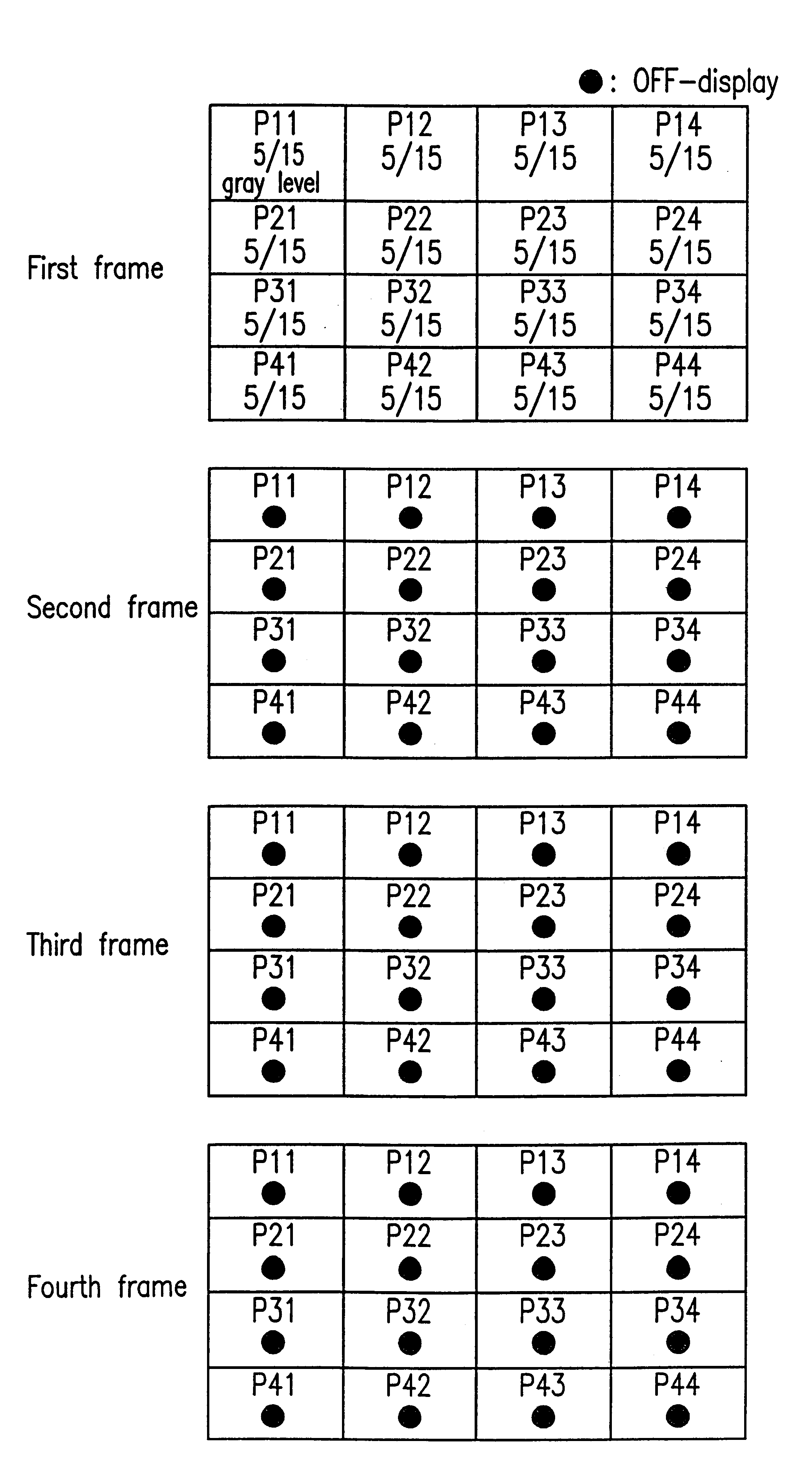
The display data converting circuit 2 receives input display data S101 containing a plurality of bits, and divides the input display data S101 into binary display data S201 and gray scale display data S202 in such a manner as to enable pulse width mo...

example 2

(Example 2)

FIG. 4A shows an example configuration of a display device 200 according to Example 2 of the present invention. FIG. 4B is a flowchart illustrating the operation of the display device 200.

A control circuit 150A of the display device 200 of Example 2 includes a display data converting circuit 2A which performs pulse width modulation one pixel in a plurality of adjacent pixels in a row instead of the display data converting circuit 2 of the control circuit 150 as shown in FIG. 1.

The display data converting circuit 2A receives input display data S101 containing a plurality of bits, and divides the input display data S101 into binary display data S201 and gray scale display data S202 in such a manner as to enable pulse width modulation one pixel in a plurality of adjacent pixels in a row. The display data converting circuit 2A switches between the binary display data S201A and the gray scale display data S202A for each frame and outputs either of them to the display data sign...


PUM

PropertyMeasurementUnit
threshold voltageaaaaaaaaaa
voltageaaaaaaaaaa
scanning voltageaaaaaaaaaa

Abstract

A control circuit for use in a display device capable of displaying gray scale including a plurality of column electrodes and a plurality of row electrodes intersecting each other and pixels provided around the intersections thereof, includes a display data converting section for receiving input display data, dividing the input display data into binary display data and gray scale display data in such a manner as to enable pulse width modulation one frame in a plurality of frames, and outputting the binary display data and the gray scale display data: a pulse controlling section for determining the timing of applying a voltage to each of the plurality of column electrodes for the gray scale display data; and a column electrode driving section for applying a voltage corresponding to the gray scale display data to at least one said column electrode based on the timing of applying a voltage determined by the pulse controlling section.

Description

BACKGROUND OF THE INVENTION1. Field of the InventionThe present invention relates to a control circuit and a control method for a matrix type display device capable of providing gray scale display.2. Description of the Related ArtA matrix type display device is used in various office automation equipment such as personal computers and word processors, multimedia information terminals, audio-visual equipment, game machines, and the like. Recently, a matrix type display device which can provide gray scale display is often used.To provide gray scale, a frame modulation system or a pulse width modulation system is widely used in a control circuit of a conventional display device.In the frame modulation system, a constant ON or OFF display voltage which is to be applied to each pixel is selected in a frame-by-frame basis, depending on a gray level which the pixel is to display. The gray level of a pixel is determined by the temporal average of the number of frames at which the ON display...

Claims


Application Information

Patent Timeline
Patent Type & Authority Patents(United States)
IPC IPC(8): G02F1/133G02F1/13G09G5/02G09G3/36G09G3/20
CPCG09G3/2051G09G3/2014G09G3/3611
Inventor YASUNISHI, NORIOSATOH, FUTOSHI
Owner SHARP KK
Why Eureka
Try Eureka