
Deep power down control circuit

a control circuit and power supply technology, applied in the direction of information storage, static storage, digital storage, etc., can solve the problems of difficult control of reference voltage generators or power up circuits, inability to control specific power circuits, and power consumption reduction, so as to reduce unnecessary power consumption

Inactive Publication Date: 2005-02-01
SK HYNIX INC
View PDF5 Cites 38 Cited by
  • Summary
  • Abstract
  • Description
  • Claims
  • Application Information

AI Technical Summary

Benefits of technology

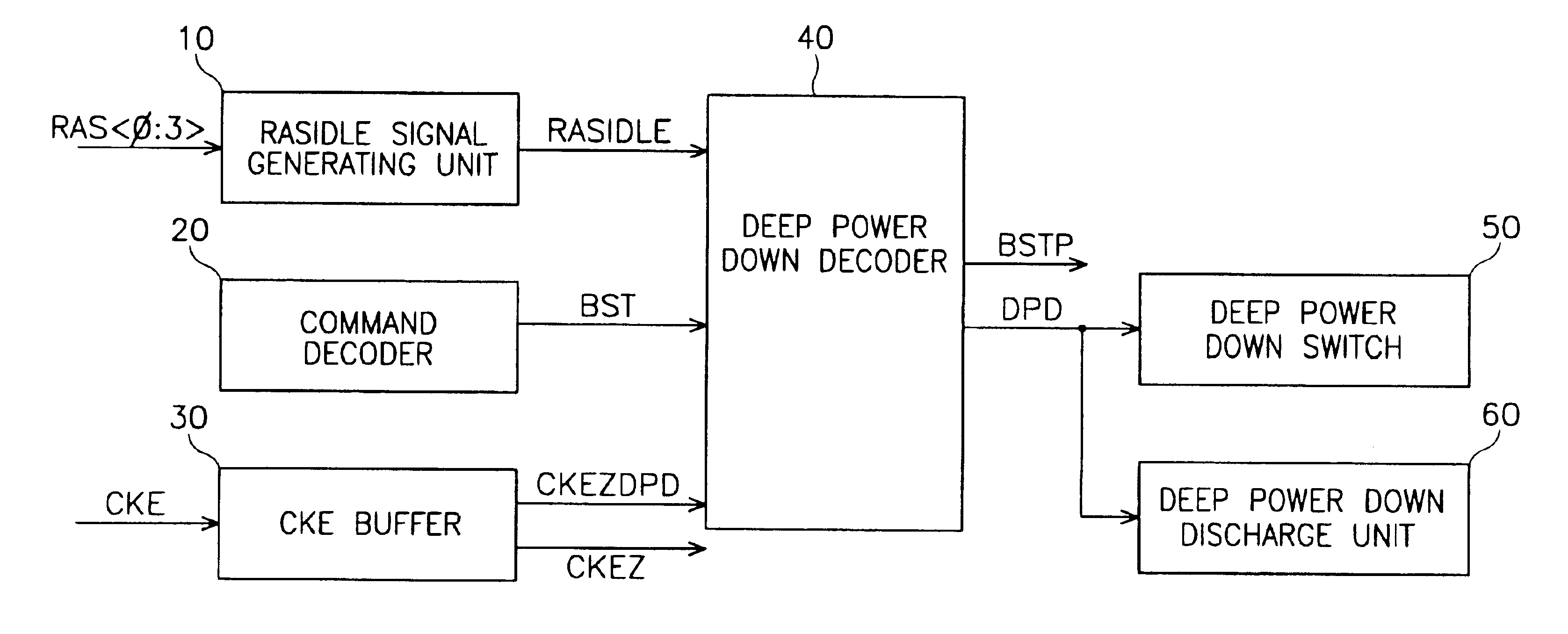
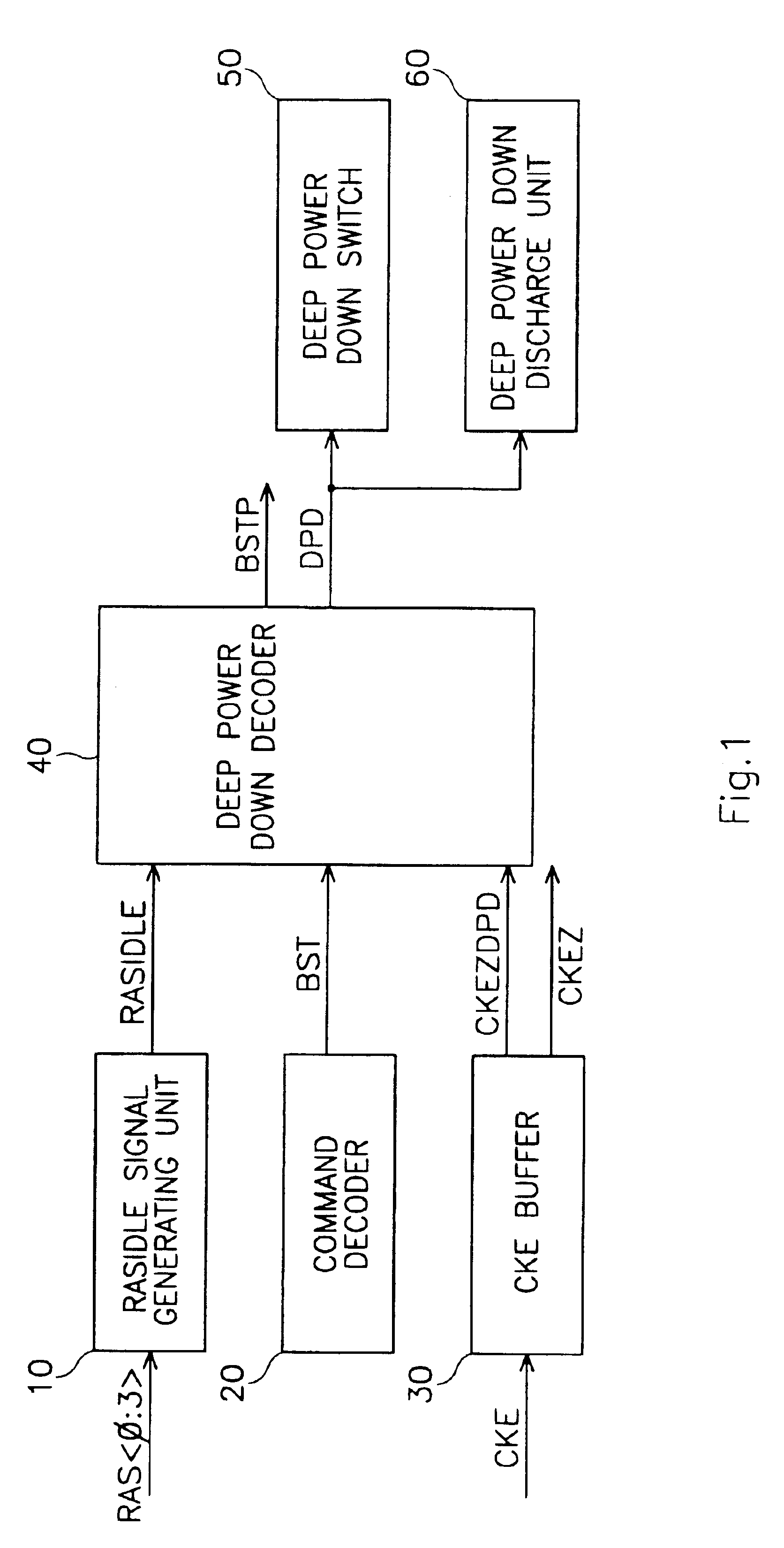
[0007]A deep power down control circuit is described herein. The disclosed deep power down control circuit reduces unnecessary power consumption by intercepting and discharging a selected one of a plurality of internal power lines. The deep power down control circuit may include: a deep power down switch unit to separate an external power voltage line from the selected one of the plurality of internal power voltage lines according to a deep power down signal; a deep power down discharge units to connect the plurality of internal power voltage lines and discharge them to a ground voltage level according to the deep power down signal; and a deep power down signal generating units, controlled according to a bank active detect signal and a burst end command, to output the deep power down signal by using a clock enable signal.

Problems solved by technology

However, the aforementioned method restrictively reduces power consumption, and thus cannot control a specific power circuit which may generate mis-operation.
For example, a reference voltage generator or power up circuit is difficult to control.
Accordingly, the semiconductor memory device fails to stop the operation of such circuits, but intercepts power of some controllable circuits.
As a result, it is difficult to reduce unnecessary power consumption sufficiently.
In particular, conventional semiconductor memory devices cannot effectively control a micro bridge generated between internal circuits or between wires.

Method used


Image

  • Deep power down control circuit
  • Deep power down control circuit
  • Deep power down control circuit

Examples


Embodiment Construction

and 5b are detailed circuit diagrams illustrating a deep power down switch;

[0014]FIG. 6 is a detailed circuit diagram illustrating a level shifter of FIG. 5b; and

[0015]FIG. 7 is a detailed circuit diagram illustrating a deep power down discharge unit of FIG. 1.

DETAILED DESCRIPTION

[0016]The present disclosure will be described in detail by way of a preferred embodiment with reference to the accompanying drawings.

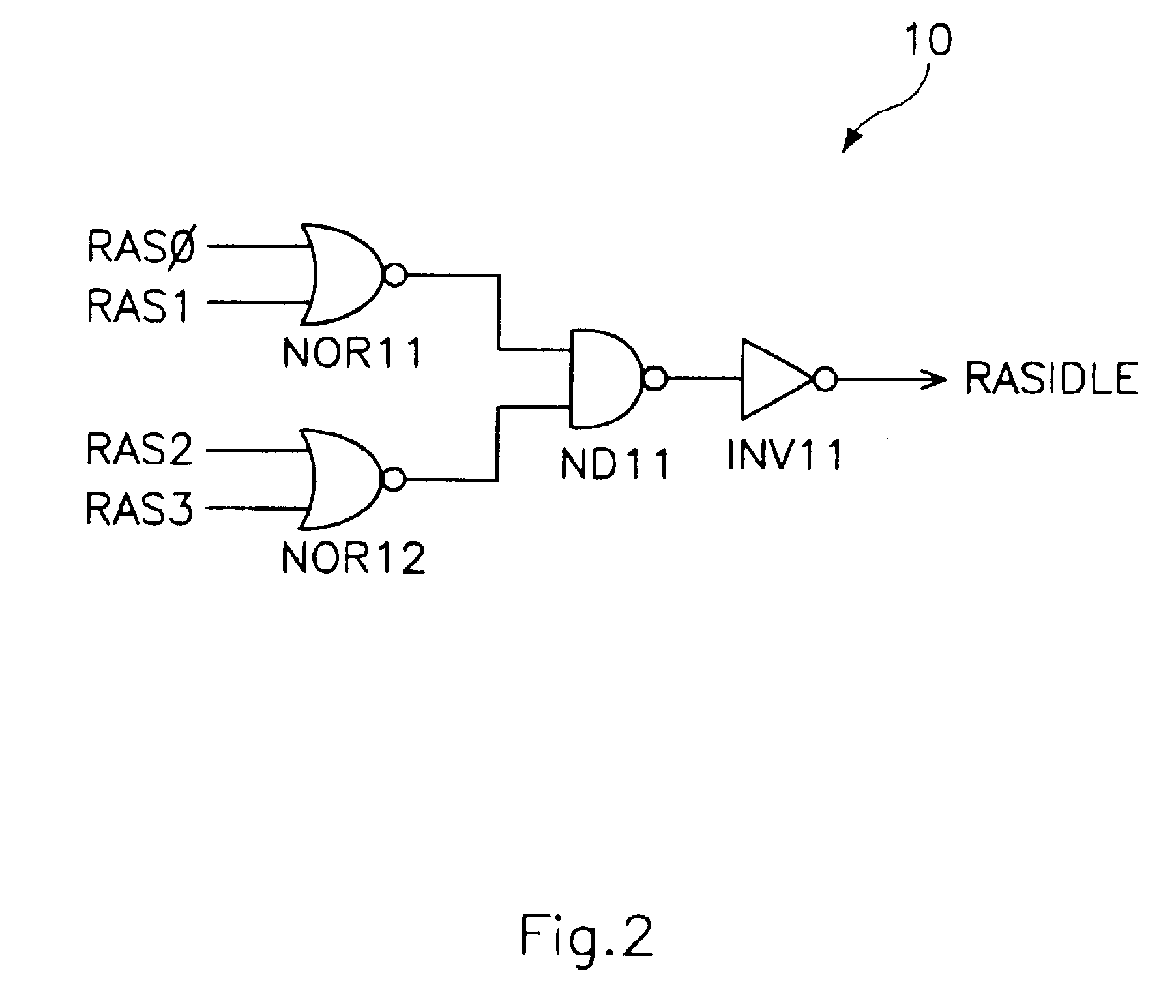
[0017]FIG. 1 is a block diagram illustrating a deep power down control circuit that includes a RASIDLE signal generating unit 10 for generating a state signal RASIDLE that is enabled when all banks are in an idle state, a command decoder 20 for generating a burst end command BST, and a CKE buffer 30 for buffering a clock enable signal CKE. Also included is a deep power down decoder 40 which receives the state signal RASIDLE, the burst end command BST and a deep power down clock enable signal CKEZDPD. The deep power down decoder 40 outputs a burst end signal BSTP in a bank act...


PUM


Abstract

A deep power down control circuit includes a deep power down switch unit to separate an external power voltage line from a selected one of a plurality of internal power voltage lines according to a deep power down signal, a deep power down discharge unit for connecting the plurality of internal power voltage lines to a ground voltage line and to discharge them to a ground voltage level according to the deep power down signal. The deep power down control circuit also includes a deep power down signal generating unit control according to a bank active detect signal and a burst end command, to output the deep power down signal by using a clock enable signal. The deep power down control circuit connects the plurality of internal power voltage lines to the ground voltage line, and thus prevents floating to remove the possibility of inversion of the power voltage or generation of the latch-up. Moreover, the deep power down control circuit prevents leakage current by a micro bridge among the plurality of internal power voltage lines.

Description

TECHNICAL FIELD[0002]The present patent relates to a deep power down control circuit for a semiconductor memory device, and in particular to an improved deep power down control circuit which can cut off a micro bridge generated between internal circuits or between wires by using a deep power down discharge circuit.BACKGROUND[0003]In general, a semiconductor memory device enables peripheral circuits to store data or externally output the stored data in an active state, and disables unnecessary peripheral circuits in a standby state to minimize power consumption. When the semiconductor memory device is maintained in the standby state for a long time, it enters into a deep power down mode to stop the operation of the peripheral circuits to reduce power consumption.[0004]The deep power down mode is controlled according to an external command in the semiconductor memory device. That is, the semiconductor memory device enters into or ends the deep power down mode according to a state of s...

Claims


Application Information

Patent Timeline
Patent Type & Authority Patents(United States)
IPC IPC(8): G11C5/14G11C11/407
CPCG11C5/147G11C5/14
Inventor PARK, KEE TEOK
Owner SK HYNIX INC
Learn More