Liquid crystal display device and a method of manufacturing a viewing angle compensation film for the same

a liquid crystal display and compensation film technology, applied in the direction of optics, polarising elements, instruments, etc., can solve the problems of defective uneven illumination of liquid crystal display devices, etc., and achieve the effect of improving viewing angle and stable multi-domain structur

Inactive Publication Date: 2005-02-08
LG DISPLAY CO LTD
View PDF8 Cites 106 Cited by
  • Summary
  • Abstract
  • Description
  • Claims
  • Application Information

AI Technical Summary

Benefits of technology

An advantage of the present invention is to provide a liquid crystal display (LCD) device having a stable multi-domain structure and an improved viewing angle by forming first and second compensation films that have a plurality of triangle patterns and includes a material having a negative anisotropy of refractive index respectively on outer surfaces of first and second substrates.
Another advantage of the present invention is to provide a method for manufacturing a viewing angle compensation film for a liquid crystal display (LCD) device by pressing a compensation film material including a material having a negative anisotropy of refractive index with a patterned mask having a plurality of triangle patterns.
Additional features and advantages of the invention will be set forth in the description which follows, and in part will be apparent from the description, or may be learned by practice of the invention. These and other advantages of the invention will be realized and attained by the structure particularly pointed out in the written description and claims hereof as well as the appended drawings.
To achieve these and other advantages and in accordance with the purpose of the present invention, as embodied and broadly described, a liquid crystal display (LCD) device includes first and second substrates, the first and second substrates having a plurality o

Problems solved by technology

Accordingly, a viewing angle property of the liquid crystal display (LCD) device is not good and thus the observer perceives that a luminance of the

Method used


Image

  • Liquid crystal display device and a method of manufacturing a viewing angle compensation film for the same
  • Liquid crystal display device and a method of manufacturing a viewing angle compensation film for the same
  • Liquid crystal display device and a method of manufacturing a viewing angle compensation film for the same

Examples


first embodiment

FIG. 3 is a plan view of a liquid crystal display (LCD) device having a two-domain structure according to the present invention. In FIG. 3, a gate line 212 is formed in a first direction and a data line 222 is formed in a second direction substantially perpendicular to the first direction. The gate and data lines 212 and 222 define a pixel region “P” by crossing each other. A thin film transistor “T” is formed at a crossing portion of the gate and data lines 212 and 222. A pixel electrode 226 connected to the thin film transistor “T” is formed in the pixel region “P”. In addition, an auxiliary electrode 224 is formed around the pixel electrode 226 in the pixel region “P”. That is, the pixel region “P” may be defined as a region substantially enclosed by the auxiliary electrode 224. The auxiliary electrode 224 is spaced apart from the adjacent gate line 212, the data line 222 and the pixel electrode 226. However, the auxiliary electrode 224 may be partially overlapped with the gate l...

second embodiment

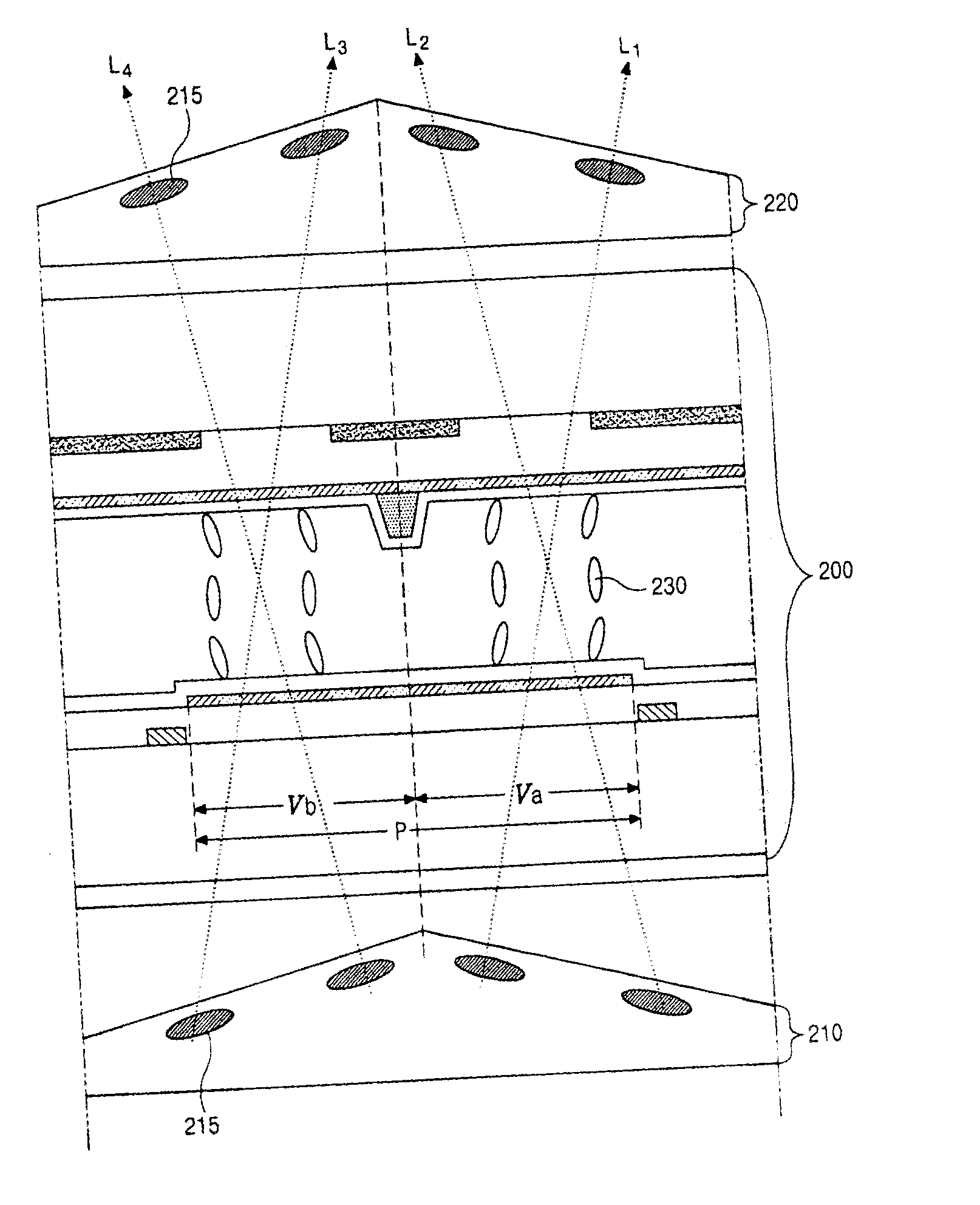
FIG. 5 is a cross-sectional view of a liquid crystal display (LCD) device having a two-domain structure and a compensation film according to the present invention. An explanation about the same elements as those in FIG. 4 will be omitted for convenience of explanation. In FIG. 5, first and second compensation films 210 and 220 are formed respectively on outer surfaces of a liquid crystal display panel 200 having a two-domain structure. The first and second compensation films 210 and 220 respectively have oblique side having a certain angle with respect to a bottom surface of the first and second compensation films 210 and 220, and discotic liquid crystal molecules 215 in the first and second compensation films 210 and 220 are arranged along the oblique sides of the first and second compensation films 210 and 220. As illustrated in FIG. 5, the first and second compensation films 210 and 220, respectively, have a shape of an isosceles triangle and vertices 210a and 220a of the first a...

third embodiment

FIG. 7 is a plan view of a liquid crystal display (LCD) device having a two-domain structure according to the present invention. In FIG. 7, a gate line 412 is formed in a first direction and a data line 422 is formed in a second direction substantially perpendicular to the first direction. The gate and data lines 412 and 422 define a pixel region “P” by crossing each other. A thin film transistor “T” is formed at a crossing portion of the gate and data lines 412 and 422. A pixel electrode 426 connected to the thin film transistor “T” is formed in the pixel region “P”. In addition, an auxiliary electrode 424 is formed around the pixel electrode 426 in the pixel region “P”. That is, the pixel region “P” may be defined as a region substantially enclosed by the auxiliary electrode 424. The auxiliary electrode 424 is spaced apart from the adjacent gate line 412, the data line 422 and the pixel electrode 426. However, the auxiliary electrode 424 may be partially overlapped with the gate l...


PUM


Abstract

A liquid crystal display (LCD) device include: first and second substrates, the first and second substrates having a plurality of pixels divided into at least two domains; a liquid crystal layer between the first and the second substrates, the liquid crystal layer having a different alignment direction in each domain; and first and second compensation films on outer surfaces of the first and second substrates, the first and second compensation films having a negative refractive anisotropy and having a triangle pattern.

Description

This application claims the benefit of Korean Patent Application No. 2002-86104, filed on Dec. 28, 2002 in Korea, which is hereby incorporated by reference for all purposes as if fully set forth herein.BACKGROUND OF THE INVENTION1. Field of the InventionThe present invention relates to a liquid crystal display (LCD) device and more particularly, to a liquid crystal display (LCD) device having a structure for improving a viewing angle and a method for manufacturing the same.2. Discussion of the Related ArtIn general, a liquid crystal display (LCD) device has upper and lower substrates spaced apart from and opposed each other, and a liquid crystal layer interposed therebetween. The upper and lower substrates respectively have an electrode thereon to form an electric field between the upper and lower substrates. The electric field formed between the upper and lower substrates aligns liquid crystal molecules so that an image can be displayed by a changing light transmittance according t...

Claims


Application Information

Patent Timeline
IPC IPC(8): G02F1/1337G02F1/13G02F1/1333G02F1/1335G02B5/30G02F1/13363G02F1/139
CPCG02F1/133632G02F1/133753G02F1/133707G02F1/1335
Inventor KIM, DO-SUNGMOON, SEUNG-JUNKIM, DO-YEON
Owner LG DISPLAY CO LTD
Why Eureka
Try Eureka