Multi-channel memory architecture

a memory architecture and multi-channel technology, applied in the field of memory systems, can solve the problems of system designers creating a variety of expensive and often complicated hierarchical memory techniques, timing problems of signals on channel output, and the performance of dram not keeping pace with density changes

Inactive Publication Date: 2005-02-08
RAMBUS INC
View PDF14 Cites 187 Cited by
  • Summary
  • Abstract
  • Description
  • Claims
  • Application Information

AI Technical Summary

Problems solved by technology

However, DRAM performance has not maintained pace with these density changes, since access times have decreased by a factor of approximately five.
This disparity between the speed of the microprocessors and the access time associated with DRAMs has forced system designers to create a variety of expensive and often complicated hierarchical memory techniques, such as SRAM (static random access memory) caches and parallel arrays of DRAMs.
Some high performance graphics systems rely on expensive frame buffers to provide the necessary bandwidth for communicating with the memory devices.
Similarly,...

Method used


Image

  • Multi-channel memory architecture
  • Multi-channel memory architecture
  • Multi-channel memory architecture

Examples


Embodiment Construction

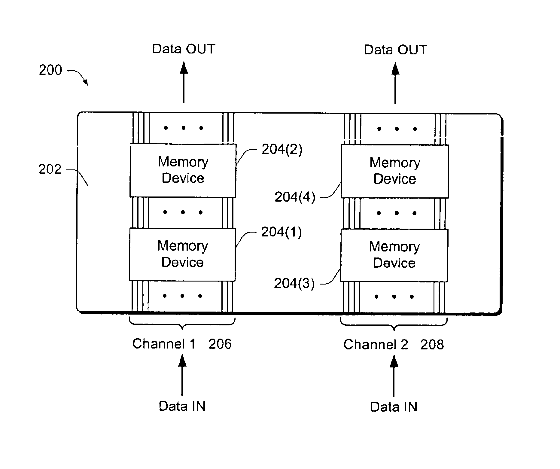
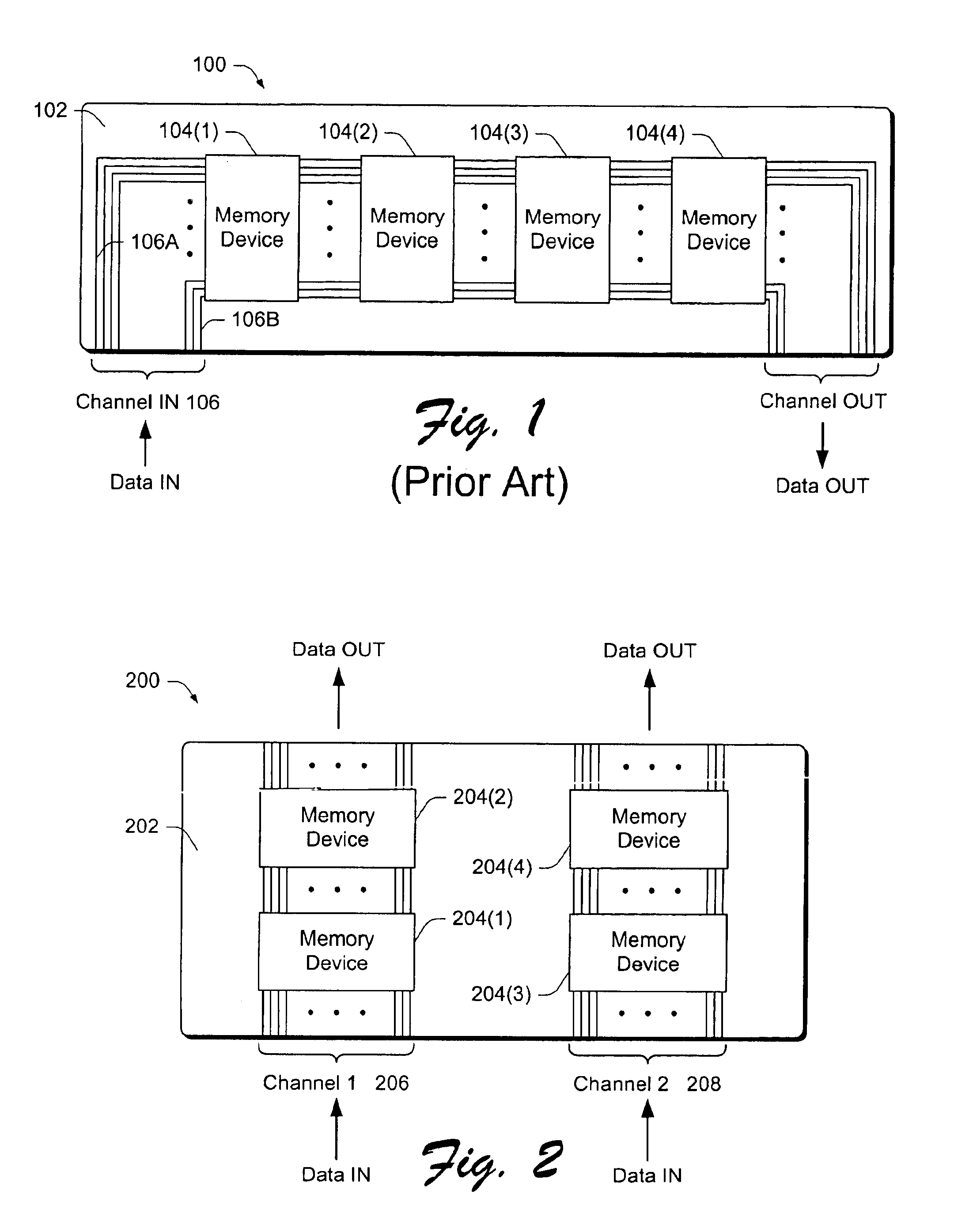
The multi-channel memory architecture described herein provides increased bandwidth by providing additional communication channels on each memory module. These additional channels increase the overall bandwidth of the memory module. Additionally, the described memory architecture routes the channel conductors such that each channel has conductors of substantially equal length. This routing of the channel conductors simplifies the layout of the conductors on the substrate and eliminates the need for special timing consideration caused by channel conductors of unequal length.

FIG. 2 illustrates another memory module 200 having multiple channels in which all channel conductors are substantially the same length. Memory module 200 eliminates the ninety degree bend in the channel conductors, thereby eliminating the associated problems, such as the timing problems caused by channel conductors of different length. Additionally, memory module 200 provides for two separate channels 206 and 208...


PUM


Abstract

A memory architecture includes a first substrate containing multiple memory devices and a first channel portion extending across the first substrate. The architecture further includes a second substrate containing multiple memory devices and a second channel portion extending across the second substrate. A connector couples the first channel portion to the second channel portion to form a single channel. The connector includes a first slot that receives an edge of the first substrate and a second slot that receives an edge of the second substrate. Another connector has a pair of slots that receive opposite edges of the first and second substrates. The channel portions extend across the substrates in a substantially linear path. Each channel portion includes multiple conductors having lengths that are approximately equal.

Description

TECHNICAL FIELDThe present invention relates to memory systems and, in particular, to a multi-channel memory architecture that provides increased communication bandwidth and provides communication channels having conductors of substantially equal length.BACKGROUNDIn recent years, DRAM (dynamic random access memory) technology has progressed dramatically. Device storage capacities have increased from 1 Kbits per chip to 64 Mbits per chip, a factor of 64,000. However, DRAM performance has not maintained pace with these density changes, since access times have decreased by a factor of approximately five. During this same time period, microprocessor performance has increased by several orders of magnitude. This disparity between the speed of the microprocessors and the access time associated with DRAMs has forced system designers to create a variety of expensive and often complicated hierarchical memory techniques, such as SRAM (static random access memory) caches and parallel arrays of...

Claims


Application Information

Patent Timeline
IPC IPC(8): H05K7/02G11C5/00H05K1/14
CPCG11C5/00H05K1/14H05K2201/10159
Inventor HABA, BELGACEMKHALILI, SAYEHMULLEN, DONALD R.GAMINI, NADER
Owner RAMBUS INC
Why Eureka
Try Eureka