Process for producing printed circuits and printed circuits thus obtained

a technology of printed circuits and printed circuits, which is applied in the direction of resist details, final product manufacturing, and high current circuit adaptations, etc., can solve the problems of inability to increase the transverse cross-sectional dimensions of the track, the application of these auxiliary conductive strips currently requires a lot of manual labor, and the design can offer sufficient resistance. , to achieve the effect of more economical

Inactive Publication Date: 2005-02-22
POWER ONE ITAL
View PDF34 Cites 1 Cited by
  • Summary
  • Abstract
  • Description
  • Claims
  • Application Information

AI Technical Summary

Benefits of technology

The objective of the present invention is the provision of a process for mounting auxiliary conductive elements on printed circuits, which is simpler, more economical and faster than the conventional systems.
A further objective of the present invention is the provision of a process which allows simple and economical production of printed circuits of different types without the necessity of dimensioning the auxiliary conductive elements in a specific and dedicated manner for each individual circuit.
A further objective of the present invention is the provision of a printed circuit with auxiliary conductive elements which is cheaper and simpler than conventional circuits.
The invention is therefore based on the idea of manipulating the auxiliary conductive elements as if they were normal SMD technology electronic components. This allows mounting to be enormously simplified since the auxiliary conductive elements are also applied by the automatic machines in the same phase of application of the SMD components.
The auxiliary conductive elements are preferably mutually identical so as to achieve the maximum standardisation of the process. However, the use also of different dimensions, or at least of a few different dimensional standards, on the same circuit, is not excluded. These may consist of metal pads of substantially rectangular outline of limited height, and may be produced from copper or some other highly conductive metal or metal alloy and may possibly be coated with a suitable metallic layer which facilitates the adhesive bonding and subsequent soldering. For example, the auxiliary conductive elements may have a forge tinning treatment or the like, with the objective also of preventing oxidation thereof during storage.

Problems solved by technology

In this manner, the design can offer sufficiently limited resistance and avoid excessive heating.
However, both of the dimensions of the transverse cross-section of a track cannot be increased at will for several reasons.
The application of these auxiliary conductive strips currently requires an appreciable input of manual labour.

Method used


Image

  • Process for producing printed circuits and printed circuits thus obtained
  • Process for producing printed circuits and printed circuits thus obtained
  • Process for producing printed circuits and printed circuits thus obtained

Examples


Embodiment Construction

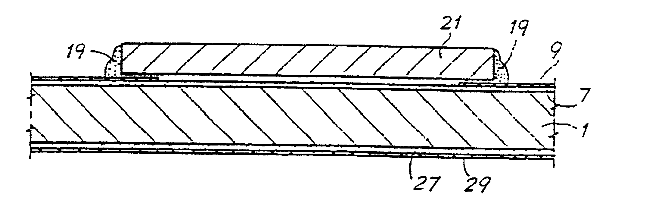
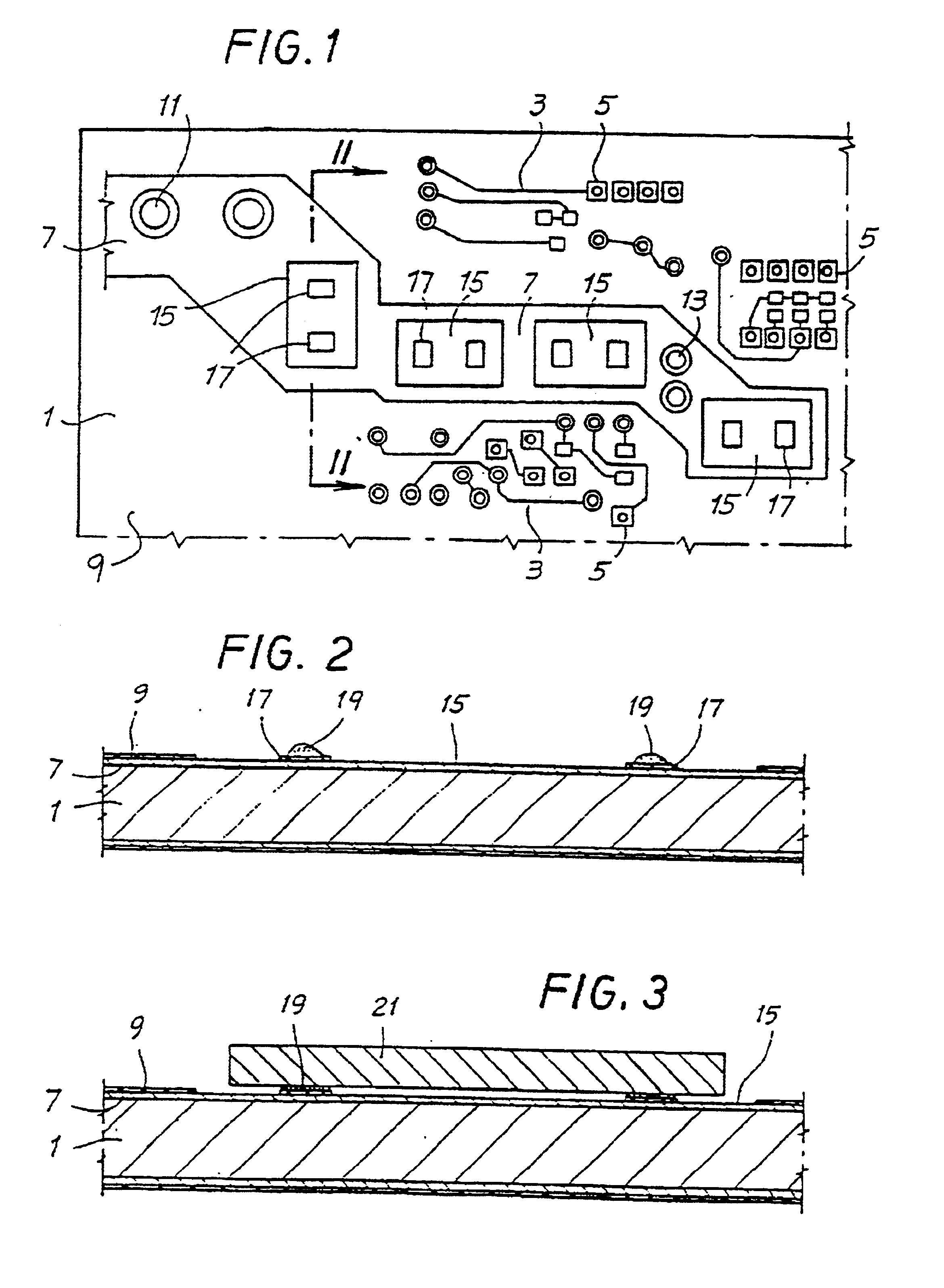
FIG. 1 shows, purely as a simplified example, a portion of laminar support board 1 for making printed circuits by the process according to the invention. The laminar support 1 includes electrically conductive tracks 3 and 7 and lands 5. The tracks 3 and 7 can be constructed as small tracks 3 or large tracks 7. The laminar support 1 also includes holes 11 and 13 for mounting electronic components and may be covered by a layer of solder-resist 9. As shown in FIG. 1, the tracks 3 and 7 may include uncovered zones 15 as locations without the layer of the solder resist 9. For one method of the present invention, these zones 15 will include areas 17 which are shown as solder-resist islands 17.

FIG. 2 shows a greatly magnified transverse cross-section on II—II of FIG. 1 of the portion of laminar support 1 of FIG. 1. The arrangement of the conductive tracks 3 and 7, of the holes 11 and 13 and of the lands 5 for applying the SMD components is purely random and merely has the objective of faci...


PUM

PropertyMeasurementUnit
thicknessaaaaaaaaaa
conductiveaaaaaaaaaa
electrical conductivityaaaaaaaaaa

Abstract

There is described a process for producing printed circuits comprising a laminar support, an electrically conductive track on the laminar support, and an auxiliary conductive element soldered to the conductive track. There is a provision to apply the auxiliary conductive element by means of an apparatus for applying SMD components.

Description

BACKGROUND OF THE INVENTIONThe present invention relates to a process for producing printed circuits comprising a laminar support or board, on which is produced a plurality of electrically conductive tracks for connecting a plurality of electronic components. More particularly this invention relates to a novel technique for applying auxiliary conductive elements to the laminar support board, having the objective of increasing the conductivity of the tracks at specified points in the circuit, where the power components are located. The invention also relates to a printed circuit obtained by this novel process as well as to a loader of auxiliary conductive elements which is produced so as to be used with a process according to the invention.State of The ArtThe prior art teaches the producing electronic circuits with laminar supports or boards produced from “vetronite” or equivalent materials. The boards include, on one or both faces, one or more tracks of conductive material. Copper i...

Claims


Application Information

Patent Timeline
Patent Type & Authority Patents(United States)
IPC IPC(8): H05K3/34H05K3/30H05K1/02
CPCH05K1/0263H05K3/305H05K3/341H05K3/3452H05K2201/099Y10T29/49144H05K2201/1028H05K2201/1084H05K2203/0588Y10T29/4913Y10T29/53178H05K2201/10272Y02P70/50
Inventor CANOVA, ANTONIO
Owner POWER ONE ITAL
Why Eureka
Try Eureka