Force detector

a detector and force technology, applied in the field of force detectors, can solve the problems of disadvantageous power consumption of force detectors using capacitance elements, large power consumption during operation, and inability to efficiently suppress power consumption

Inactive Publication Date: 2005-02-22
WAKO CO LTD
View PDF59 Cites 53 Cited by
  • Summary
  • Abstract
  • Description
  • Claims
  • Application Information

AI Technical Summary

Benefits of technology

[0011]The object of the invention is, therefore, to provide a force detector using capacitance elements or variable resistance elements wherein power consumption can be efficiently suppressed.

Problems solved by technology

However, general C / V converter circuits and C / f converter circuits have oscillation circuits inside, so that power consumption during operation is relatively great.
Therefore, if conventional force detectors using such capacitance elements are installed into various electronic apparatuses, power consumption increases as a whole.
Therefore, a force detector using a capacitance element is disadvantageous in terms of power consumption although it is advantageous in terms of manufacturing costs.
However, even by taking this measure, wasteful power consumption cannot be completely suppressed.
Considering the actual use pattern of a portable telephone or the like, the period of input operation for cursor movements or the like is very short, so that operation of circuits with great power consumption while an operator does not carry out operational inputs at all is not efficient.
However, to measure the electric resistance of the resistor, it is necessary to make a current flow in the resistor, and some degree of power consumption is inevitable during the measurement.
Therefore, if the abovementioned force detector using the variable resistance element is installed into various electronic apparatuses, power consumption increases as a whole.

Method used


Image

  • Force detector
  • Force detector
  • Force detector

Examples


Embodiment Construction

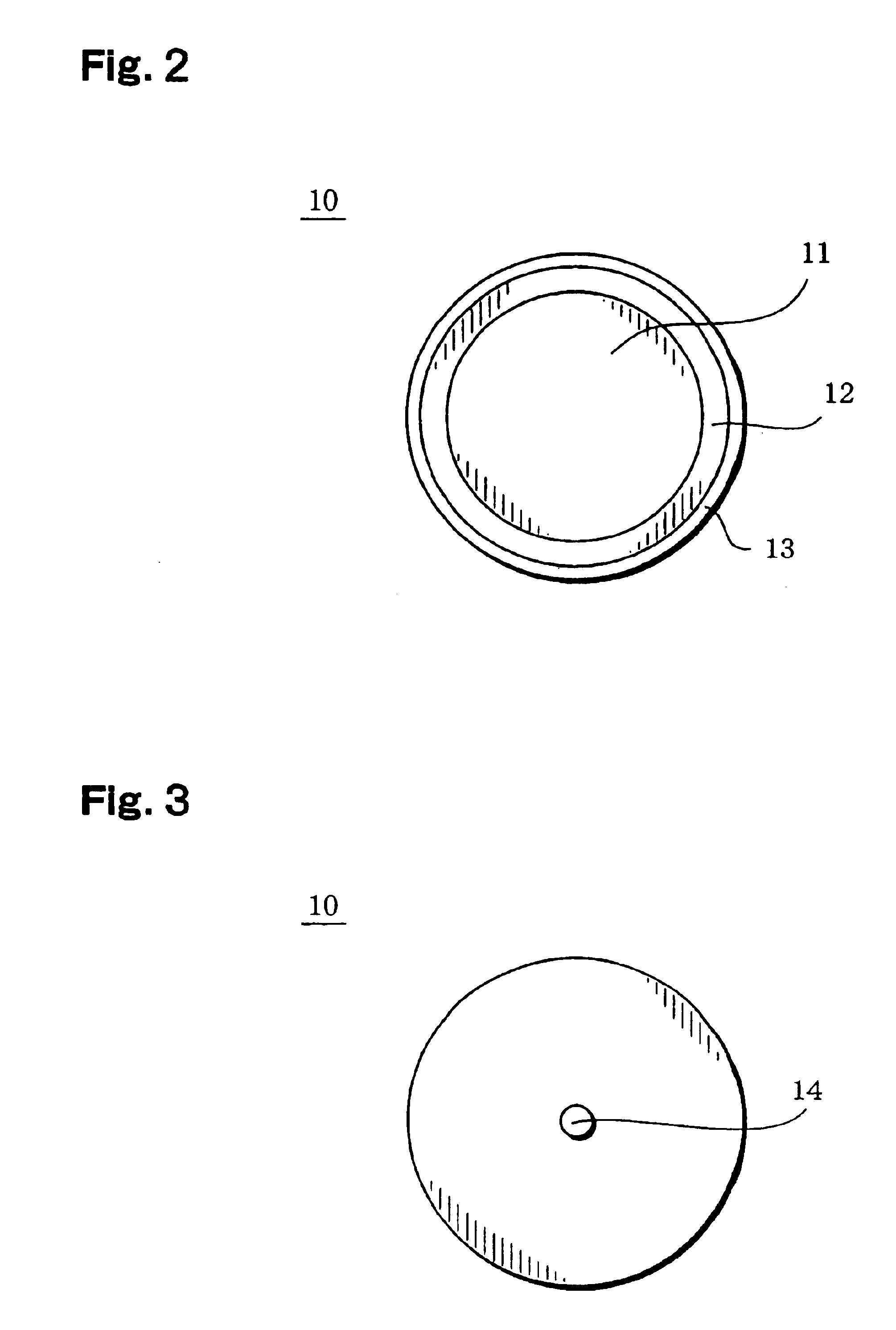
"d_n">[0098]FIG. 22 is a top view of substrate 40A to be used as an input device for an electronic apparatus which has only a one-dimensional operational input function;

[0099]FIG. 23 is a top view of substrate 40B to be used as an input device for an electronic apparatus having a three-dimensional operational input function and a clicking function;

[0100]FIG. 24 is a top view of substrate 40C to be used as an input device for an electronic apparatus having a three-dimensional operational input function;

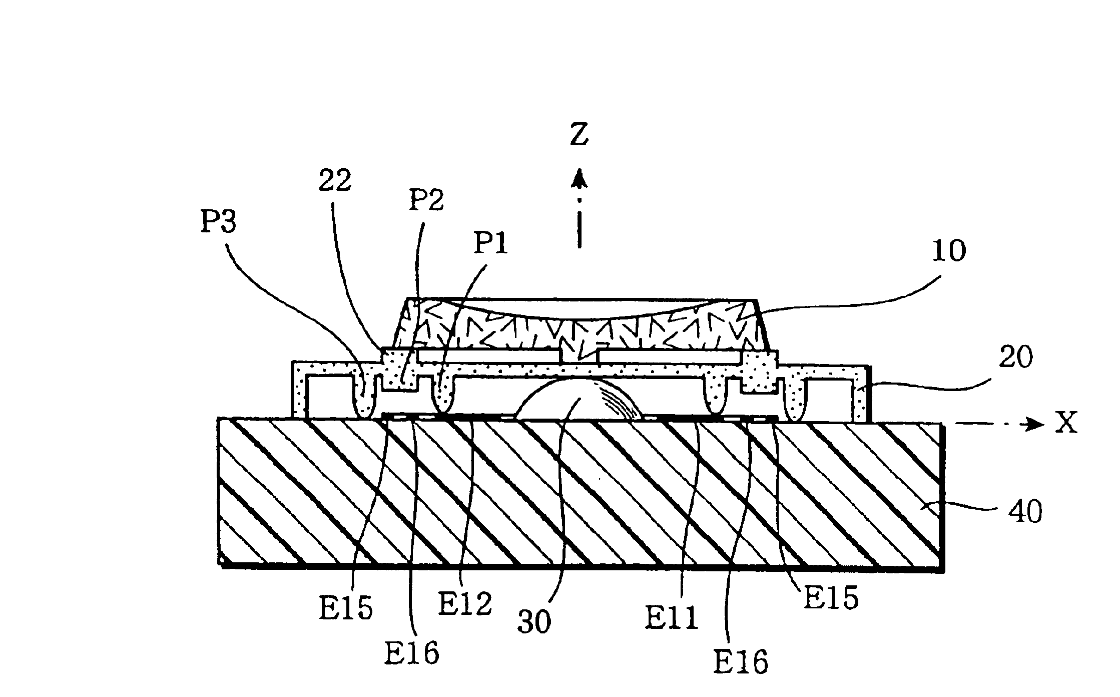
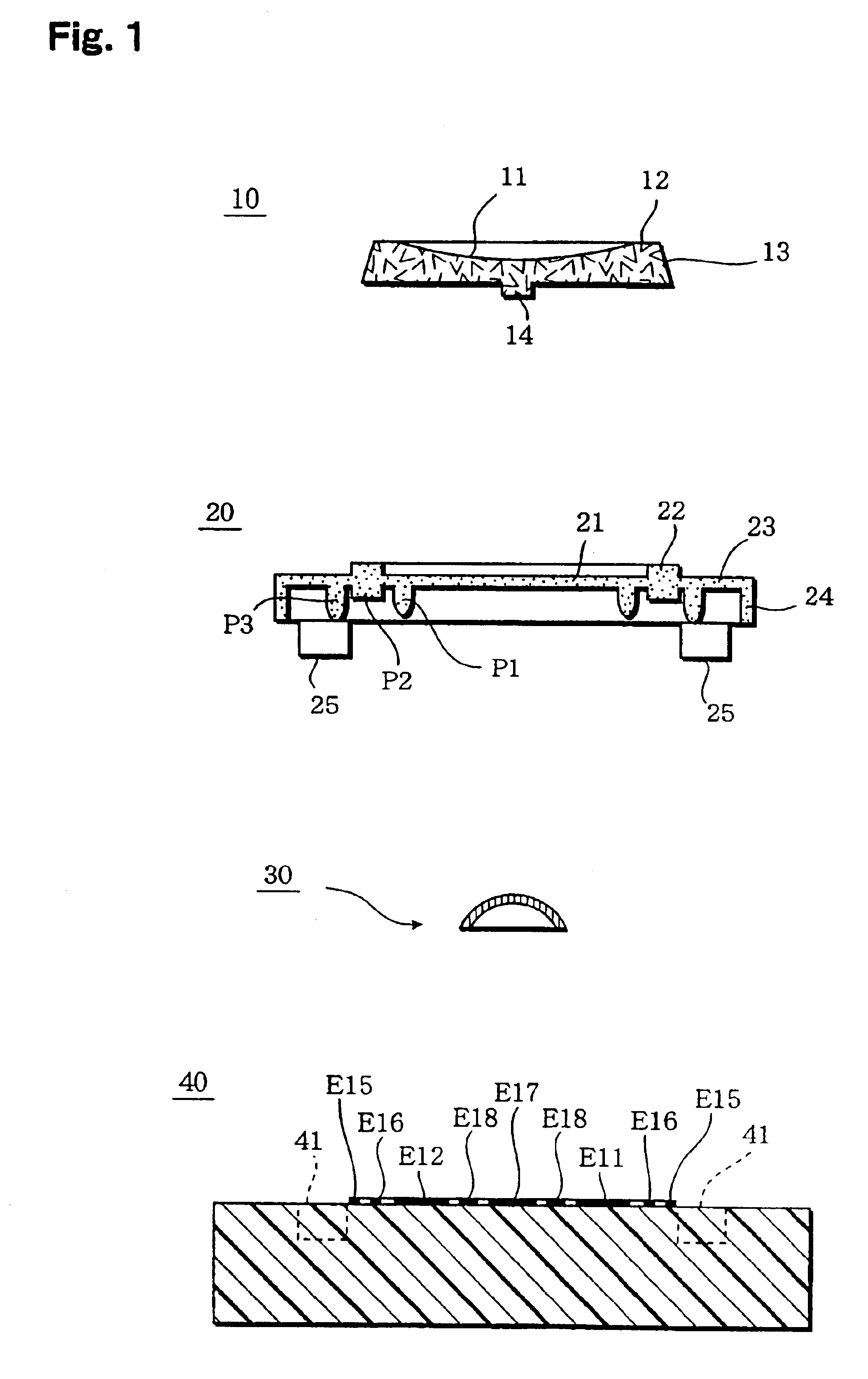
[0101]FIG. 25 is an exploded side sectional view of an input device for an electronic apparatus using a plurality of domed structures;

[0102]FIG. 26 is a bottom view of elastic deformable body 20D, a side section along the center of which is shown in FIG. 25;

[0103]FIG. 27 is a bottom view showing displacing conductive layer 26 formed on the lower surface of the elastic deformable body 20D shown in FIG. 26;

[0104]FIG. 28 is a top view of the substrate 40D, a side section along the center ...


PUM


Abstract

The invention provides a force detector in which power consumption is suppressed. Four electrodes E11 through E14 are formed on a substrate, and an elastic deformable body formed of a rubber film is disposed thereon. A conductive coating is applied on the lower surface of the elastic deformable body to provide a displacing conductive layer 26. Four capacitance elements C11 through C14 are comprised by the electrodes E11 through E14 and the displacing conductive layer 26 opposed to the electrodes. The capacitance values thereof are converted into voltage values V11 through V14 by C/V converter circuit 50, and based on operation by signal processing circuit 60, an external force applied to the elastic deformable body is detected. A pair of contacting electrodes E15 and E16 are formed on the substrate, and when an external force with a predetermined strength or more is applied, the elastic deformable body deforms, and the displacing conductive layer 26 comes into contact with both electrodes E15 and E16, simultaneously. The potential of the electrode E16 is taken-in from the terminal T5, and when said potential is Vcc, the C/V converter circuit 50 is operated in a standby mode with less power consumption, and when said potential is GND, the circuit is operated in a normal mode.

Description

[0002]“This application is a divisional of copending application Ser. No. 10 / 022,580 filed on Dec. 17, 2001, claims the benefit thereof and incorporates the same by reference.”BACKGROUND OF THE INVENTION[0003]The present invention relates to a force detector using capacitance elements or variable resistance elements and, more specifically, to a force detector suitable for being applied to an input device which obtains operational inputs indicating predetermined operation amounts into an electronic apparatus such as a portable telephone, game machine, or the like which executes predetermined processing based on predetermined programs.[0004]In an electronic apparatus such as a portable telephone, game machine, or the like, a predetermined operational input by a user is accepted, and based on this operational input, an execution of program proceeds. Normally, such an operational input is accepted while a user looks at a cursor or other objects displayed on a display screen, and an inpu...

Claims


Application Information

Patent Timeline
Patent Type & Authority Patents(United States)
IPC IPC(8): H03K17/94H03K17/975H01H25/04
CPCG01L1/142G01L5/165G01L5/223H01H25/041H03K17/975H01H2239/006H01H2239/078H01H2300/022H01H2205/024
Inventor OKADA, KAZUHIROTANIGUCHI, NOBUMITSU
Owner WAKO CO LTD
Why Eureka
Try Eureka