Semiconductor memory device utilizing tunnel magneto resistive effects and method for manufacturing the same

a tunnel magneto resistive effect and memory device technology, applied in the field of magnetic random access memory (mram), can solve the problems of insufficient resistance r variation, inability to secure a sufficient mr ratio, and the accompanying memory utilizing this conventional tmr elemen

Inactive Publication Date: 2005-03-01
KK TOSHIBA
View PDF16 Cites 13 Cited by
  • Summary
  • Abstract
  • Description
  • Claims
  • Application Information

AI Technical Summary

Benefits of technology

According to a first aspect of this invention, there is provided a semiconductor memory device, which comprises: first memory elements to store a first state or a second state according to a change in resistance value, each of the first memory elements comprising one terminal and the other terminal, the first memory elements arranged parallel with each other; a first wiring connected with the one terminal of each of the first memory elements; and a second wiring formed in parallel with the first wiring and connected with the other terminal of each of the first memory elements; wherein the first state or the second state stored in one of selected from the first memory elements is read out by delivering an electric current from one of the first and second wirings via the one of selected from the first memory elements to the other of the first and second wirings.

Problems solved by technology

The MRAM memory utilizing this conventional TMR element is accompanied with the following problems.
However, since the MR ratio reported to date is at most 50% or so, the variation of resistance ΔR cannot be made sufficiently large.
Therefore, it becomes impossible to secure a sufficient MR ratio, thereby making it difficult to employ the differential sense amplifier system.
However, this conventional structure is accompanied with a problem that since the units 73 are employed for constituting a single memory cell 76, four elements, i.e. two TMR elements 71+two of MOS transistors 72 are required to be included in each bit of the memory cell 76, this conventional structure is disadvantageous in increasing the area of the memory cell 76.
Additionally, even though it is certainly possible to double the margin for determining the “1” and “0” data, it can not necessarily be said that a sufficient margin can be secured for reading data.

Method used


Image

  • Semiconductor memory device utilizing tunnel magneto resistive effects and method for manufacturing the same
  • Semiconductor memory device utilizing tunnel magneto resistive effects and method for manufacturing the same
  • Semiconductor memory device utilizing tunnel magneto resistive effects and method for manufacturing the same

Examples


first embodiment

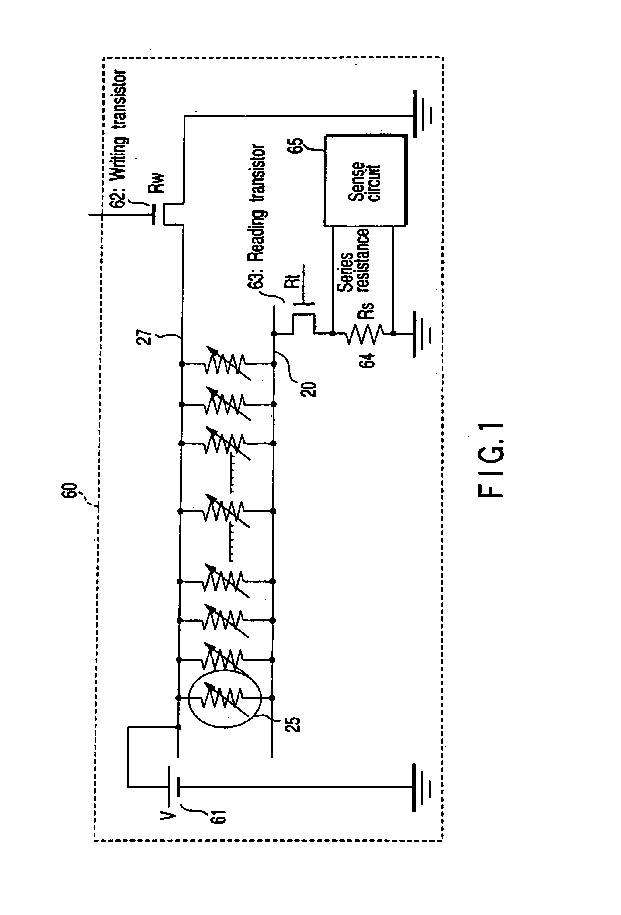
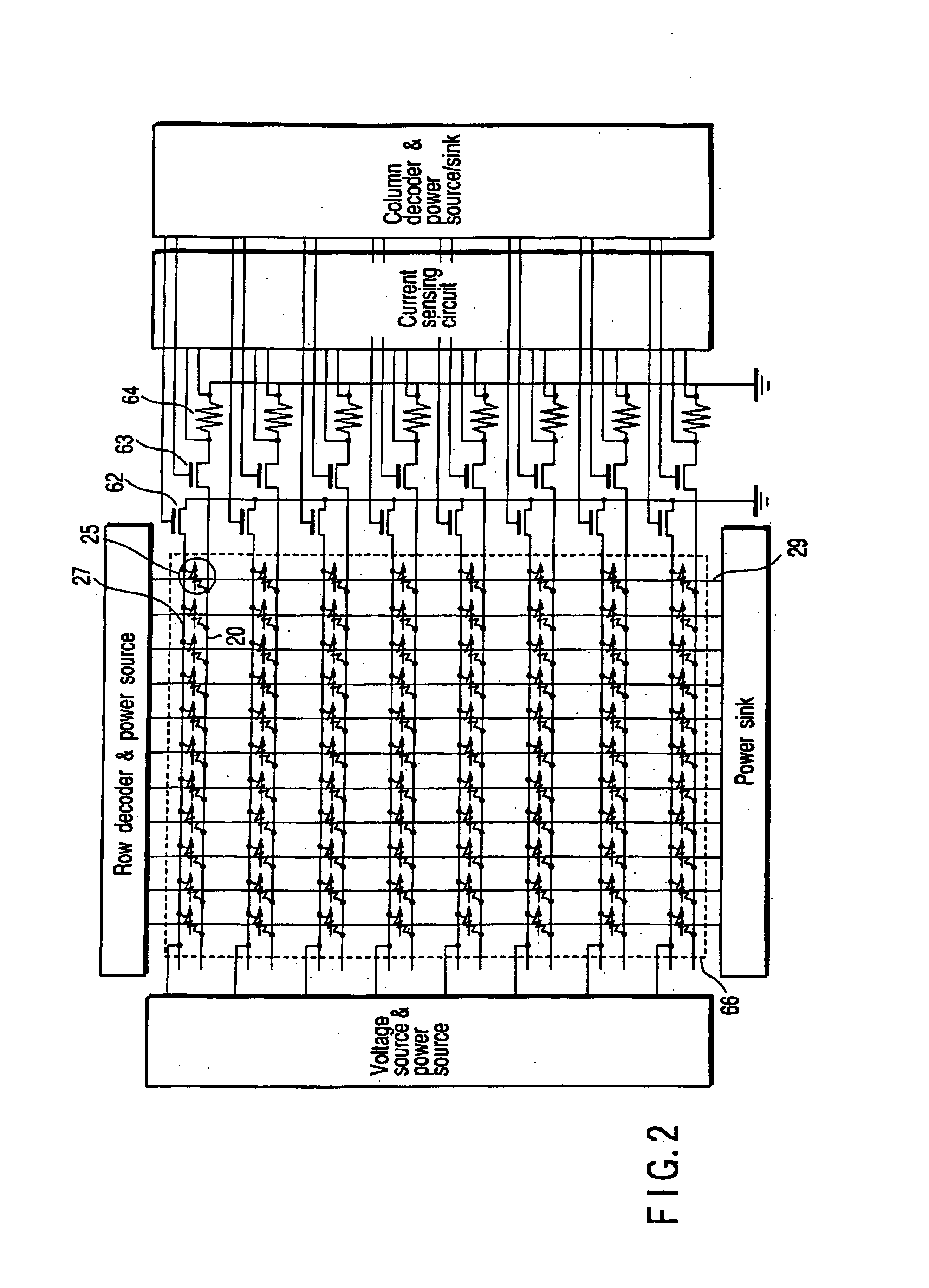
FIG. 1 shows an equivalent circuit of the semiconductor memory device according to a first embodiment of this invention, and FIG. 2 shows a block diagram of the memory cell array wherein the equivalent circuit shown in FIG. 1 is arranged one after another in parallel with each other. Next, the structure of the equivalent circuit of the semiconductor memory device according to this invention will be explained.

As shown in FIG. 1, the equivalent circuit 60 of a semiconductor memory device according to a first embodiment is constituted by a plurality of tunneling magneto resistive effect element of TMR (Tunneling Magneto Resistive) type (hereinafter referred to as TMR element) 25 which are arranged parallel with each other, an upper data transfer line 27, a lower data transfer line 20, a constant-voltage generating circuit 61, a writing transistor 62, a reading transistor 63, a series resistor 64, and a sense circuit 65.

In this case, the upper data transfer line 27 is electrically conne...

second embodiment

This second embodiment is featured in that the gate electrode of MISFET (MOSFET) is substituted for the word line employed in the aforementioned first embodiment. Incidentally, the constituent components and the principle of operation are the same as those of the first embodiment, and therefore, the explanation thereof will be omitted, and only the features which differ from the first embodiment will be explained.

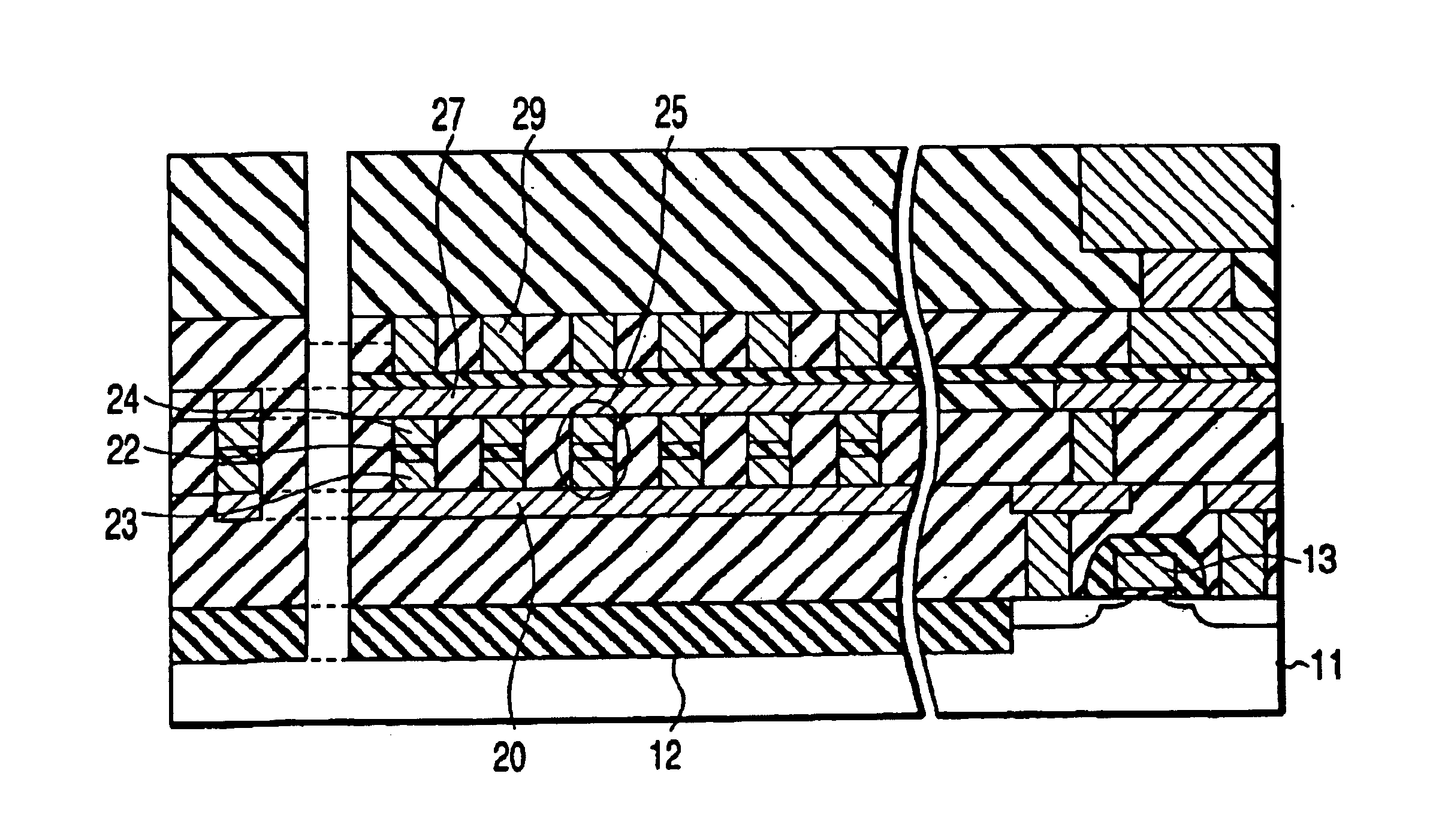
FIG. 15 shows a cross-sectional view illustrating the semiconductor memory device according to the second embodiment of this invention. As shown in FIG. 15, the semiconductor memory device according to the second embodiment employs, as a memory element, a plurality of TMR elements 25 each constituted by a first magnetic body 23, a second magnetic body 24, and an insulating layer 22 which is formed of a non-magnetic body and sandwiched between the first and second magnetic bodies 23 and 24. Further, a plurality of TMR elements 25 are arranged parallel with each other. The fi...

third embodiment

This second embodiment is featured in that the TMR elements of line-and-space configuration (linear) are formed on and along the lower data transfer line, and that the TMR elements are patterned in an island configuration by making use of a patterned upper data transfer line. Incidentally, the constituent components and the principle of operation are the same as those of the first embodiment, and therefore, the explanation thereof will be omitted, and only the features of manufacturing method which differ from the first embodiment will be explained.

FIG. 22 shows a cross-sectional view illustrating the semiconductor memory device according to the third embodiment of this invention. As shown in FIG. 22, the semiconductor memory device according to the third embodiment is the same in structure as that of the first embodiment, and therefore, the explanation thereof will be omitted.

FIGS. 23 to 29 respectively shows a cross-sectional view illustrating a manufacturing step of the semicondu...


PUM

PropertyMeasurementUnit
thicknessaaaaaaaaaa
thicknessaaaaaaaaaa
depthaaaaaaaaaa

Abstract

There is provided, according to one embodiment of this invention, a semiconductor memory device including first memory elements to store a first state or a second state according to a change in resistance value, each of the first memory elements including one terminal and the other terminal, the first memory elements arranged parallel with each other, a first wiring connected with the one terminal of each of the first memory elements, and a second wiring formed in parallel with the first wiring and connected with the other terminal of each of the first memory elements, wherein the first state or the second state stored in one of selected from the first memory elements is read out by delivering an electric current from one of the first and second wirings via the one of selected from the first memory elements to the other of the first and second wirings.

Description

BACKGROUND OF THE INVENTION1. Field of the InventionThis invention relates to a semiconductor device and the manufacturing method thereof, and in particular, to magnetic random access memory (MRAM) wherein a mechanism for storing information “1” and “0” by taking advantage of tunnel magneto resistive (TMR) effects is utilized as a memory cell, and also to the manufacturing method thereof.2. Description of the Related ArtIn recent years, there has been proposed a MRAM utilizing, as an information memory element, a tunneling magneto resistive element (hereinafter, referred to simply as a TMR element).This TMR element is formed of a structure wherein a thin tunneling insulating film is sandwiched between a couple of magnetic films. Further, this TMR element is enabled to take two states, i.e. a state wherein the directions of the spins of this couple of magnetic films are the same and parallel with each other, and another state wherein the directions of the spins of these magnetic film...

Claims


Application Information

Patent Timeline
Patent Type & Authority Patents(United States)
IPC IPC(8): H01L21/70H01L21/8246H01L27/22G11C11/14G11C11/15H01F10/32H01F41/22H01F41/32H01L27/10H01L27/105H01L43/08
CPCB82Y10/00H01L27/228H01L27/222H10B61/00H10B61/22H01L27/10
Inventor HOSOTANI, KEIJI
Owner KK TOSHIBA
Why Eureka
Try Eureka