Laser link structure capable of preventing an upper crack and broadening an energy window of a laser beam, and fuse box using the same

a laser beam and link structure technology, applied in the field of laser link structure, can solve problems such as the limitation of the area of the fuse box

Inactive Publication Date: 2005-03-01
SAMSUNG ELECTRONICS CO LTD
View PDF1 Cites 7 Cited by
  • Summary
  • Abstract
  • Description
  • Claims
  • Application Information

AI Technical Summary

Problems solved by technology

Additionally, there is a limit in reducing the area of the fuse box since the energy window of a laser beam is narrow.

Method used


Image

  • Laser link structure capable of preventing an upper crack and broadening an energy window of a laser beam, and fuse box using the same
  • Laser link structure capable of preventing an upper crack and broadening an energy window of a laser beam, and fuse box using the same
  • Laser link structure capable of preventing an upper crack and broadening an energy window of a laser beam, and fuse box using the same

Examples


Embodiment Construction

Korean Patent Application No. 2001-72985, filed Nov. 22, 2001, and entitled: “Laser Link Structure Capable of Protecting Upper Crack and Broadening Energy Window of Laser Beam, and Fuse Box Using the Same,” is incorporated by reference herein in its entirety.

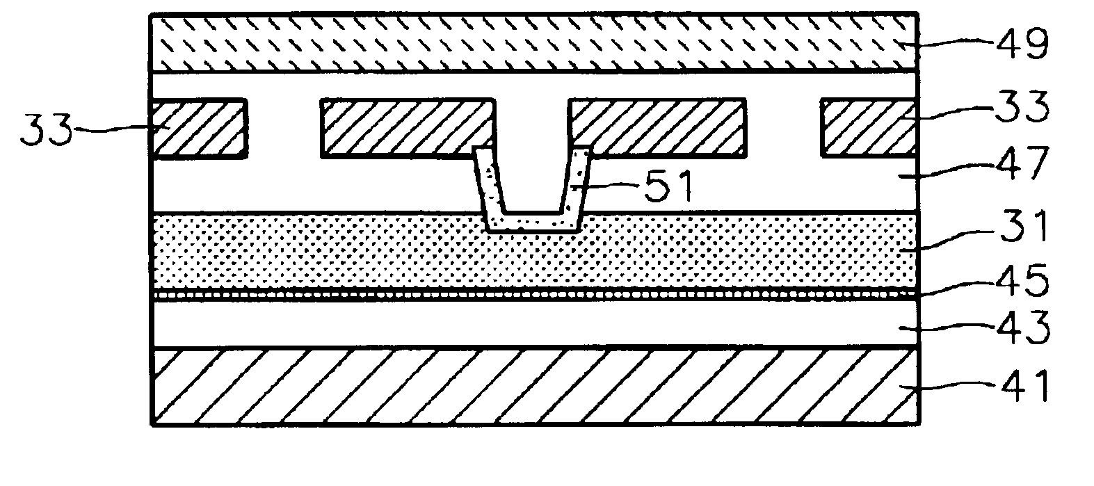
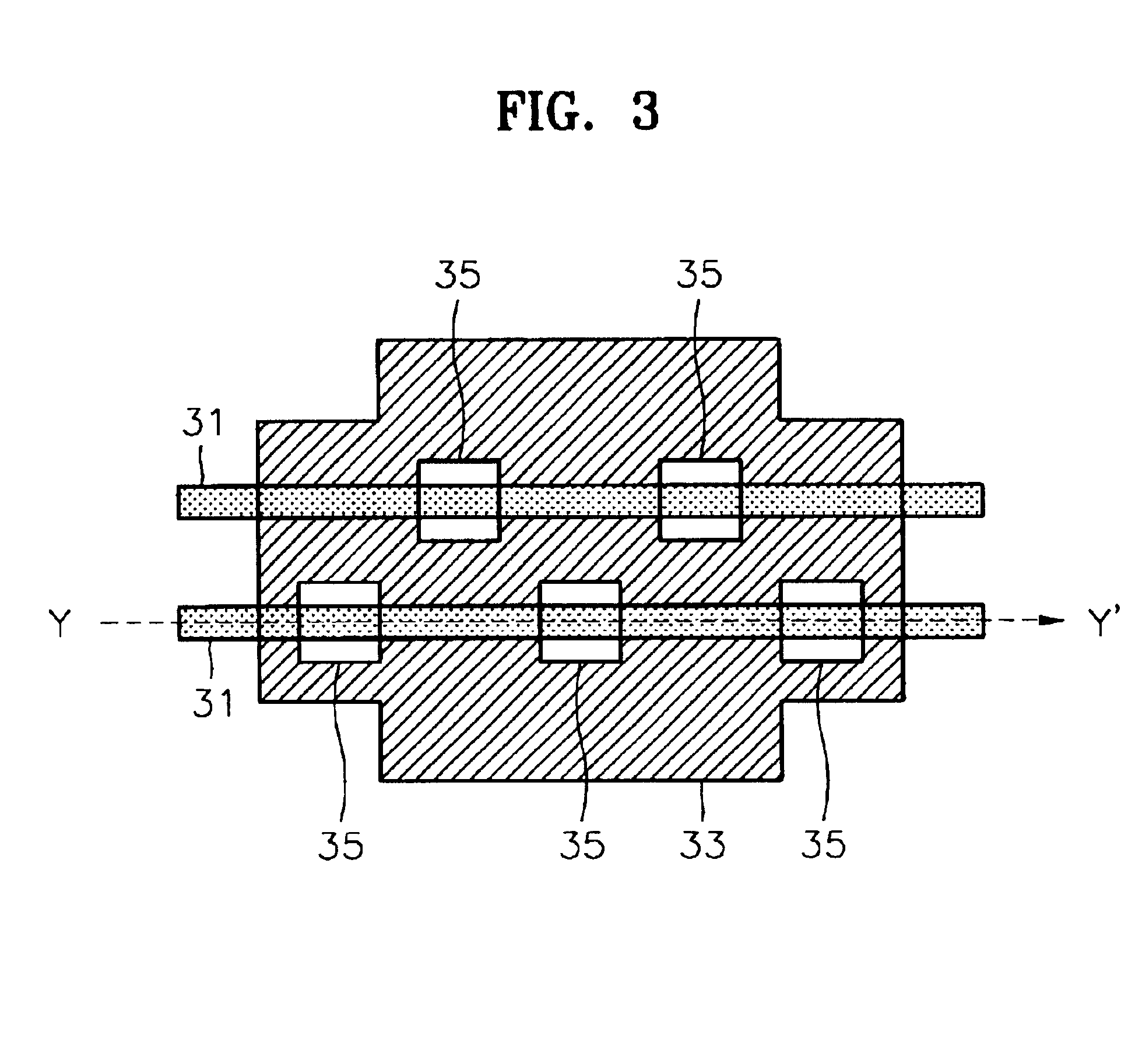
FIG. 3 illustrates a view of a preferred layout of a laser link structure according to the present invention. The laser link structure shown in FIG. 3 differs from the conventional laser link structure of FIG. 1 in that a second conductive line pattern 33 is preferably broadly formed on two or more first conductive line patterns 31 which are positioned in parallel at predetermined intervals. Further, at least one hole region 35 is preferably formed on each of the first conductive line patterns 31.

FIG. 4 illustrates a cross-sectional view of the laser link structure of FIG. 4, taken along section line Y-Y′. FIG. 5 illustrates a view of the laser link structure of FIG. 3 in which the first conductive line patterns 31 are linked wi...


PUM


Abstract

A laser link structure used in semiconductor devices and a fuse box using the laser link structure preferably include a plurality of first conductive line patterns positioned in parallel at predetermined intervals, and a second conductive line pattern broadly formed on the plurality of first conductive line patterns for forming hole regions which link the second conductive line pattern to the plurality of first conductive line patterns. Preferably, at least one hole region is formed on each of the plurality of first conductive line patterns, and via holes are formed in the hole regions.

Description

BACKGROUND OF THE INVENTION1. Field of the InventionThe present invention relates to a semiconductor device. More particularly, the present invention relates to a laser link structure used in semiconductor devices and a fuse box using the laser link structure.2. Description of the Related ArtIn general, in order to increase yield, a semiconductor device includes normal memory cell arrays and redundancy memory cell arrays, in which a normal memory cell having defects (hereinafter, ‘defective cell’) is replaced with a redundancy memory cell (hereinafter, ‘redundant cell’).As is well known in the art, a semiconductor memory device includes a redundancy circuit for replacing a defective cell with a redundant cell. The redundancy circuit includes program means for programming the address of a defective cell and a predetermined control circuit for controlling the redundancy circuit. The program means includes a plurality of fuses that decode the address of a defective cell using laser or ...

Claims


Application Information

Patent Timeline
Patent Type & Authority Patents(United States)
IPC IPC(8): H01L23/52H01L23/525G11C17/14G11C29/00G11C17/18G11C29/04H01L21/82H01L27/10
CPCG11C17/14H01L23/5258G11C29/785H01L2924/0002H01L2924/00H01L21/82
Inventor BANG, JEONG-HOSHIN, KYEONG-SEONKANG, SANG-SEOKCHOI, HO-JEONGJU, HYEN-WOOKBANG, KWANG-KYU
Owner SAMSUNG ELECTRONICS CO LTD
Why Eureka
Try Eureka